
Chao Wei, Yuping Ma, Yuan Han, Yao Zhang, Xuehui Chen. Femtosecond Laser Processing of Ultrahard Materials[J]. Laser & Optoelectronics Progress, 2019, 56(19): 190003
- Laser & Optoelectronics Progress
- Vol. 56, Issue 19, 190003 (2019)
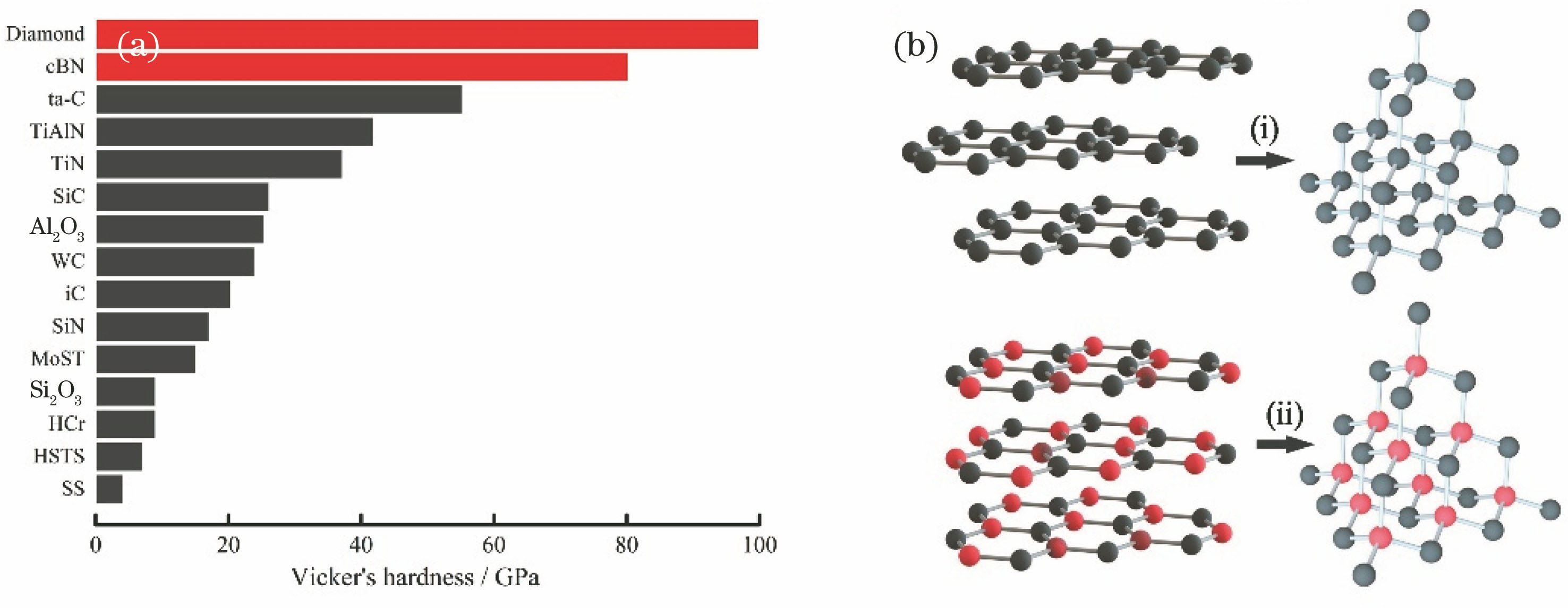
Fig. 1. Hardness and atomic structures of two typical ultrahard materials. (a) Hardness of different materials; (b) cubic crystal structures of diamond and CBN
![Timescale of physical phenomena involved in laser-material interaction[21]](/richHtml/lop/2019/56/19/190003/img_2.jpg)
Fig. 2. Timescale of physical phenomena involved in laser-material interaction[21]
Fig. 3. Schematic of difference between long-pulse laser processing and short-pulse laser processing[23]
Fig. 4. Schematics of evolution of maximum temperature of target and pulse energy incubation effect in femtosecond laser processing[26-27]. (a) Evolution of maximum temperature of target; (b) pulse energy incubation effect
Fig. 5. Functional relationship between ablation rate of diamond and laser energy density under different pulse durations
Fig. 6. Schematics of non-linear absorption and avalanche ionization mechanism[36]
Fig. 7. Fitting curve between logarithmic laser power and square of dimple diameter machined by femtosecond laser on SC diamond[25]
Fig. 8. Range of laser ablation volume (gray area)
Fig. 9. SEM photographs of polycrystalline diamond side profiles processed at different pulse energies, scanning numbers, and focusing objective magnification
Fig. 10. Common femtosecond laser processing methods for ultrahard materials. (a) Laser direct writing[48]; (b) accelerated beam[59]; (c) dry etching assistant processing[53]; (d) intensity mask projection processing[64]; (e) femtosecond laser dual-mode rapid fabrication system based on SLM[61]
Fig. 11. Micro-morphologies of ablated area obtained by femtosecond laser spot etching and line etching at different laser powers. (a)-(f) Spo tetching; (g)-(i) line etching
Fig. 12. Graphite channel arrays fabricated by femtosecond laser with energy of 4 μJ. N is number of pulses; Z is step length; side-view low-power optical micrographs illustrate continuity of graphitization channels through bulk diamond
Fig. 13. Applications of femtosecond laser direct writing. (a) Processing process of BLPCD micromilling tool, from left to right: BLPCD blank, FSPL ball forming, finished BLPCD micromilling tool; (b) SEM photograph of SC diamond plane refractive lens
Fig. 14. Applications of SLM technologies. (a)(b) Letters processed by 10 pulses on surface of polycrystalline diamond, with dotted double arrows representing direction of laser polarization; (c) letter “S” processed by 50 pulses on surface of polycrystalline diamond; (d) SEM photograph of convex SC diamond edges processed by femtosecond laser acceleration beam
Fig. 15. Material removal mechanism of nt-CBN by femtosecond laser spot etching at low power[82]
Fig. 16. nt-CBN tool. (a)(b) Blanks of nt-CBN micro-tool processed by femtosecond laser; (c) finished nt-CBN micro-tool after focused ion beam grinding
Fig. 17. Surface micro-morphologies of CBN tool fabricated by femtosecond laser and cutting experimental results of different tools under different cutting conditions (dry/wet processing). (a) Surface micro-morphologies; (b) comparison of friction coefficients of polished surface, parallel, orthogonal, and banded micro-textured tools; (c) relationship between cutting length and adhension area of different micro-textured tools; (d) atom concentration of targets on surface of different micro-textured tools
Fig. 18. Experimental results of surface adhesion degree of micro-textured tools[87]. (a) Three-dimensional profile of rake face of CBN tools after cutting experiment under different parameters, where white arrow indicates cutting adhesion area of aluminum alloy; (b) changes of cutting chips when cutting length increases to 1800 m under dry friction. Processing results marked by blue arrow and box attribute to traditional tool, while red arrow and box marked results are processed by optimum tool
Fig. 19. Relationship between cutting length and flank friction width of traditional CBN tools and micro-textured CBN tools under dry and wet conditions
|
Table 1. Properties and applications of diamond and CBN

Set citation alerts for the article
Please enter your email address
© Copyright 2018-2021 | Chinese Laser Press. All Rights Reserved 沪ICP备15018463号-20