
Zenglin Li, Ran Zuo. Simulation of Interfacial Stress in Sapphire-GaN Heterogeneous Film System[J]. Laser & Optoelectronics Progress, 2020, 57(19): 193102
- Laser & Optoelectronics Progress
- Vol. 57, Issue 19, 193102 (2020)
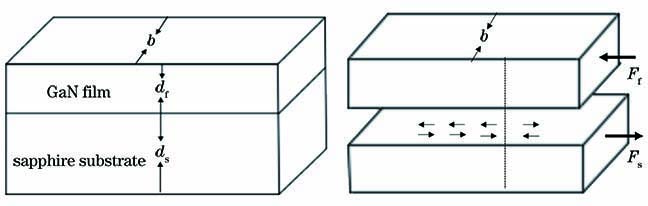
Fig. 1. Schematic of thin film system. (a) Sapphire-GaN heterogeneous film system; (b) force free body in specified interface
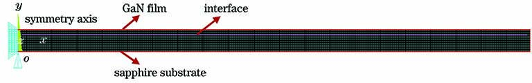
Fig. 2. Finite element model of sapphire-GaN heterogeneous film system
Fig. 3. Temperature distribution of sapphire-GaN heterogeneous film system after cooling for 1 min
Fig. 4. Warpage deformation of sapphire-GaN heterogeneous film system after cooling for 1 min
Fig. 5. von Mises stress distribution of sapphire-GaN heterogeneous film system after cooling for 1 min
Fig. 6. Interfacial stress distribution of different thicknesses of GaN films for cooling to 1073 K. (a) 2 inch substrate; (b) 4 inch substrate
Fig. 7. Variation of interfacial stress with the thickness of GaN film (ignore edges). (a) 2 inch substrate; (b) 4 inch substrate
Fig. 8. Interfacial stress distribution of different sapphire substrate thickness for cooling to 1073 K. (a) 2 inch substrate; (b) 4 inch substrate
Fig. 9. Variation of interfacial stress with ds/df. (a) 2 inch substrate; (b) 4 inch substrate
Fig. 10. Variation of the maximum warpage of film system with the thickness of GaN film. (a) 2 inch substrate; (b) 4 inch substrate
Fig. 11. Change of stress caused by lattice mismatch and thermal mismatch with cooling time
|
Table 1. Physical properties of materials[12]

Set citation alerts for the article
Please enter your email address
© Copyright 2018-2021 | Chinese Laser Press. All Rights Reserved 沪ICP备15018463号-20