• Laser & Optoelectronics Progress
  • Vol. 57, Issue 6, 061018 (2020)
Ying Xu1、*, Qingyuan Wang1, Congcong Luo1, and Sohn Hoon2
Author Affiliations
  • 1College of Civil and Environmental Engineering, Harbin Institute of Technology (Shenzhen), Shenzhen Key Lab of Urban & Civil Engineering Disaster Prevention & Reduction, Shenzhen, Guangdong 518055, China;
  • 2Department of Civil and Environmental Engineering, Korea Advanced Institute of Science and Technology, Daejeon 34708, Republic of Korea
  • show less
    DOI: 10.3788/LOP57.061018 Cite this Article Set citation alerts
    Ying Xu, Qingyuan Wang, Congcong Luo, Sohn Hoon. Chip Crack Imaging Detection Based on Line Laser Phase-Locked Thermal Imaging[J]. Laser & Optoelectronics Progress, 2020, 57(6): 061018 Copy Citation Text show less
    Overall structure diagram of linear laser phase-locked thermal imaging system for semiconductor chip detection consisting of excitation, sensing, and control units
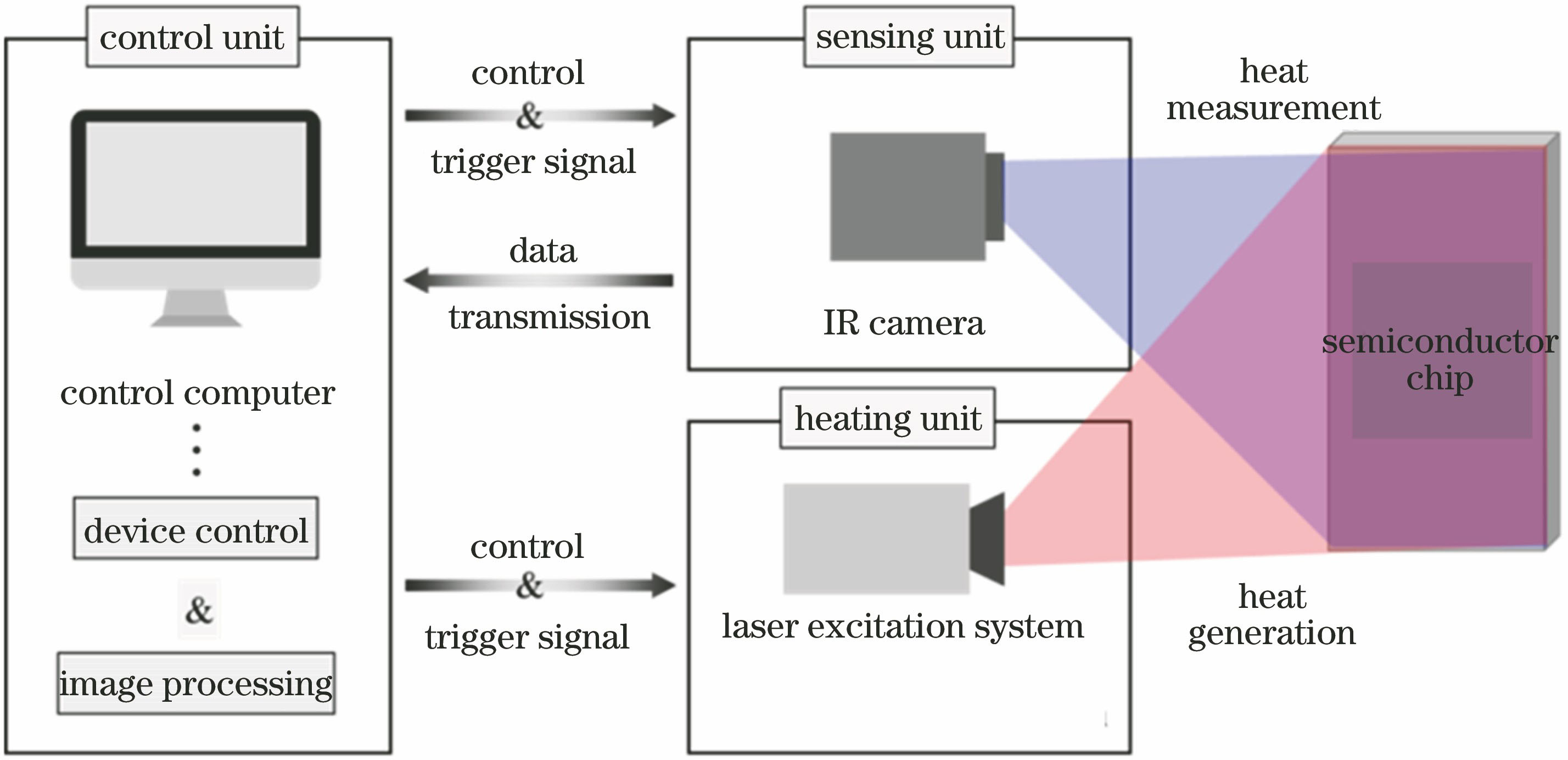
    Fig. 1. Overall structure diagram of linear laser phase-locked thermal imaging system for semiconductor chip detection consisting of excitation, sensing, and control units
    Overview of baseline-free crack visualization algorithm
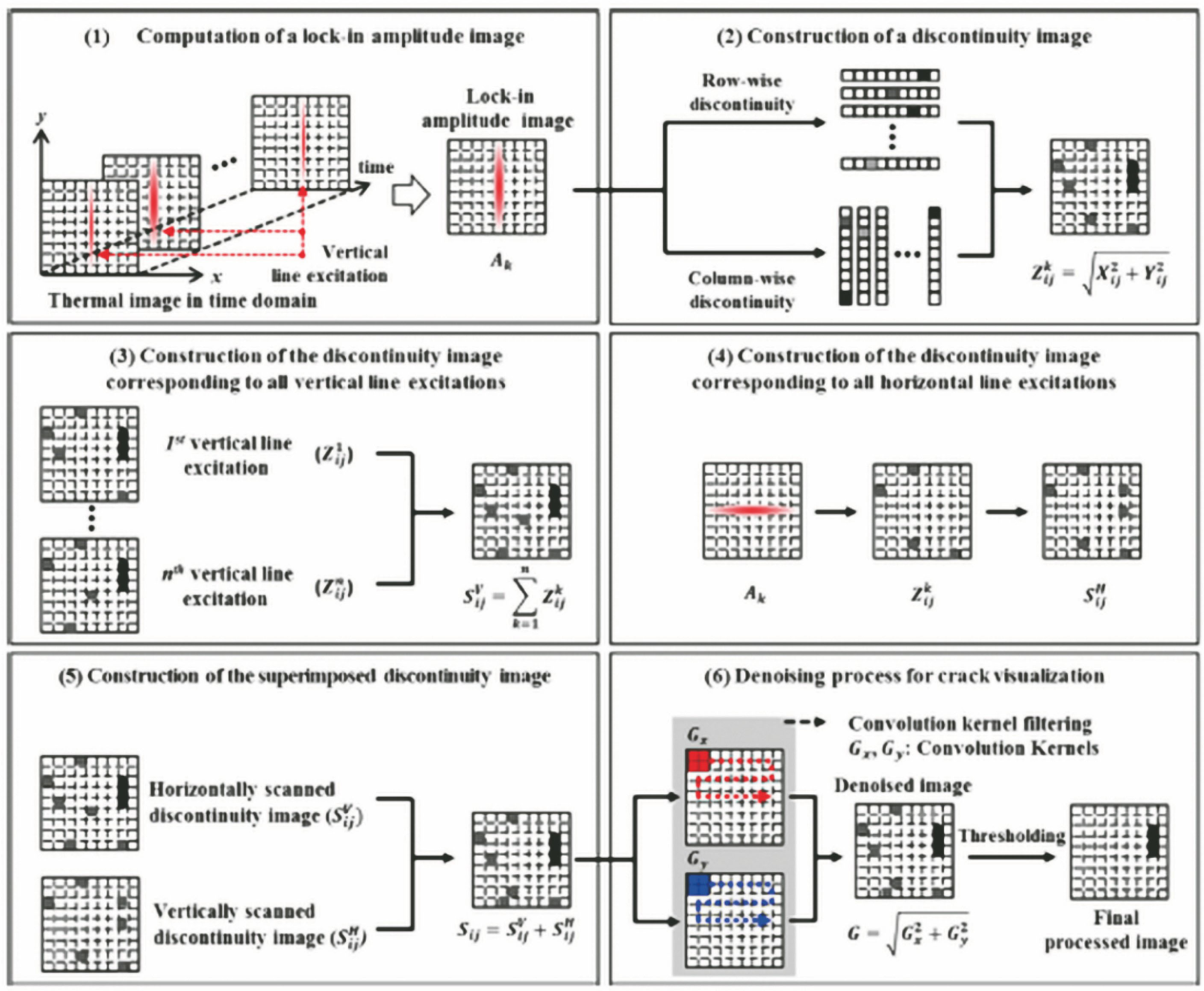
    Fig. 2. Overview of baseline-free crack visualization algorithm
    Diagrams of thermal wave generation by modulated CW laser beam and corresponding thermal response captured by IR camera. (a) Intensity of modulated CW excitation laser; (b) corresponding thermal response in time domain
    Fig. 3. Diagrams of thermal wave generation by modulated CW laser beam and corresponding thermal response captured by IR camera. (a) Intensity of modulated CW excitation laser; (b) corresponding thermal response in time domain
    Roberts cross convolution kernels. (a) Compute Kx of gradient edge at +45°; (b) compute Ky of gradient edge at -45°
    Fig. 4. Roberts cross convolution kernels. (a) Compute Kx of gradient edge at +45°; (b) compute Ky of gradient edge at -45°
    Experimental setup of linear laser phase-locked thermal imaging technology for detecting crack of semiconductor chip
    Fig. 5. Experimental setup of linear laser phase-locked thermal imaging technology for detecting crack of semiconductor chip
    Semiconductor pressed chip specimens
    Fig. 6. Semiconductor pressed chip specimens
    Microscopic images of semiconductor chip specimens with cracks. (a) Vertical cracks of pressed chip; (b) horizontal cracks of pressed chip
    Fig. 7. Microscopic images of semiconductor chip specimens with cracks. (a) Vertical cracks of pressed chip; (b) horizontal cracks of pressed chip
    Typical raw thermal images obtained from pressed chips. (a) Vertical line excitation on intact chip; (b) horizontal line excitation on intact chip; (c) vertical line excitation on vertically cracked chip; (d) horizontal line excitation on horizontally cracked chip
    Fig. 8. Typical raw thermal images obtained from pressed chips. (a) Vertical line excitation on intact chip; (b) horizontal line excitation on intact chip; (c) vertical line excitation on vertically cracked chip; (d) horizontal line excitation on horizontally cracked chip
    Raw thermal images obtained from intact chip with vertical line excitation. (a) 0 ms; (b) t (50 ms); (c) T (500 ms)
    Fig. 9. Raw thermal images obtained from intact chip with vertical line excitation. (a) 0 ms; (b) t (50 ms); (c) T (500 ms)
    Phase-locked amplitude images obtained from raw thermal images in Fig. 8. (a) Vertical line excitation on intact chip; (b) horizontal line excitation on intact chip; (c) vertical line excitation on vertically cracked chip; (d) horizontal line excitation on horizontally cracked chip
    Fig. 10. Phase-locked amplitude images obtained from raw thermal images in Fig. 8. (a) Vertical line excitation on intact chip; (b) horizontal line excitation on intact chip; (c) vertical line excitation on vertically cracked chip; (d) horizontal line excitation on horizontally cracked chip
    Discontinuous images obtained from chips. (a) Without crack; (b) with vertical crack; (c) with horizontal crack
    Fig. 11. Discontinuous images obtained from chips. (a) Without crack; (b) with vertical crack; (c) with horizontal crack
    Final images obtained after de-noising process. (a) Without crack; (b) with vertical crack; (c) with horizontal crack
    Fig. 12. Final images obtained after de-noising process. (a) Without crack; (b) with vertical crack; (c) with horizontal crack
    Ying Xu, Qingyuan Wang, Congcong Luo, Sohn Hoon. Chip Crack Imaging Detection Based on Line Laser Phase-Locked Thermal Imaging[J]. Laser & Optoelectronics Progress, 2020, 57(6): 061018
    Download Citation