
Hongyun Chen, Yu Lu, Chen Li, Xingyuan Zhao, Xiuxing Zhang, Zhixiang Zhang, Linbao Luo. Multilayer PtSe2/TiO2 NRs Schottky Junction for UV Photodetector[J]. Acta Optica Sinica, 2020, 40(20): 2025001
- Acta Optica Sinica
- Vol. 40, Issue 20, 2025001 (2020)
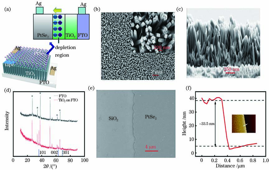
Fig. 1. Diagram of device structure and material characterization. (a) Diagram of device structure, inset shows built-in electric field at PtSe2/TiO2 surface; (b) top view SEM image of TiO2 NRs, inset shows magnification of SEM image; (c) cross-sectional view SEM image of TiO2 NRs; (d) XRD pattern of FTO and TiO2 NRs grown on FTO; (e) SEM image of PtSe2 film; (f) height profile of PtSe2 film, inset shows AFM image of PtSe2
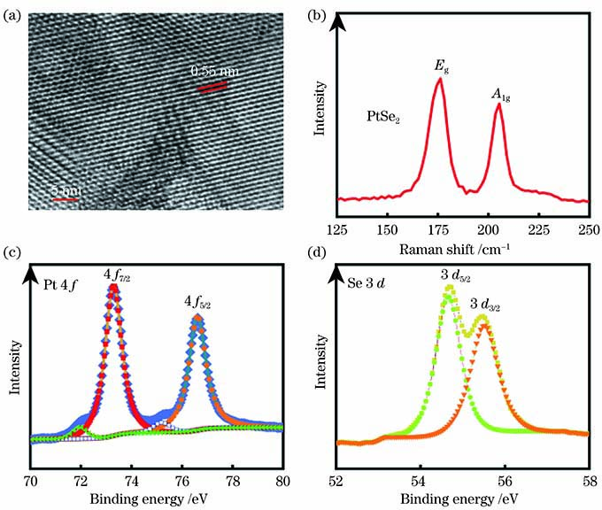
Fig. 2. Structure and composition of two-dimensional material PtSe2. (a) HRTEM image; (b) Raman spectrum; (c) XPS image of Pt 4 f; (d) XPS image of Se 3 d
Fig. 3. Response curves to 365 nm light and energy band diagram of proposed device. (a) I-V curve, inset shows I-V characteristic of dark current in logarithmic coordinates; (b) photo response under 365 nm light illumination at bias voltage of -1.0 V; (c) energy band diagram; (d) photo response of device for about two hundreds cycles of operation; (e) photo response of device before and after 5 weeks in air ambient condition
Fig. 4. Electrical performance under different optical power densities. (a) I-V curve; (b) photo response of device at bias voltage of -1.5 V; (c) fitting curve of photocurrent and optical power density; (d) relationship between Ilight/Idark and optical power density at bias voltage of -1.5 V; (e) change of responsivity and specific detection rate with incident light power density; (f) relationship between ηEQE and optical power density at bia
Fig. 5. Light absorption and response of device. (a) Spectral response of device; (b) absorption spectra of TiO2, PtSe2, and device; (c) response curve of device under 365 nm irradiation with a frequency of 1 Hz; (d) rise time and fall time of device
Fig. 6. Simple imaging of device. (a) Schematic of UV imaging system; (b) 2D current map under 365 nm light illumination
|
Table 1. Comparison of parameters of PtSe2/TiO2 NRs array photodetector and other TiO2-based heterojunction devices

Set citation alerts for the article
Please enter your email address
© Copyright 2018-2021 | Chinese Laser Press. All Rights Reserved 沪ICP备15018463号-20