Feng Liu, Fan Zhang, Hao Bian, Qing Yang, Minjing Li, Feng Chen. Development and Preparation of Refractive Infrared Microlens Array Device[J]. Laser & Optoelectronics Progress, 2020, 57(7): 071607
Search by keywords or author
- Laser & Optoelectronics Progress
- Vol. 57, Issue 7, 071607 (2020)
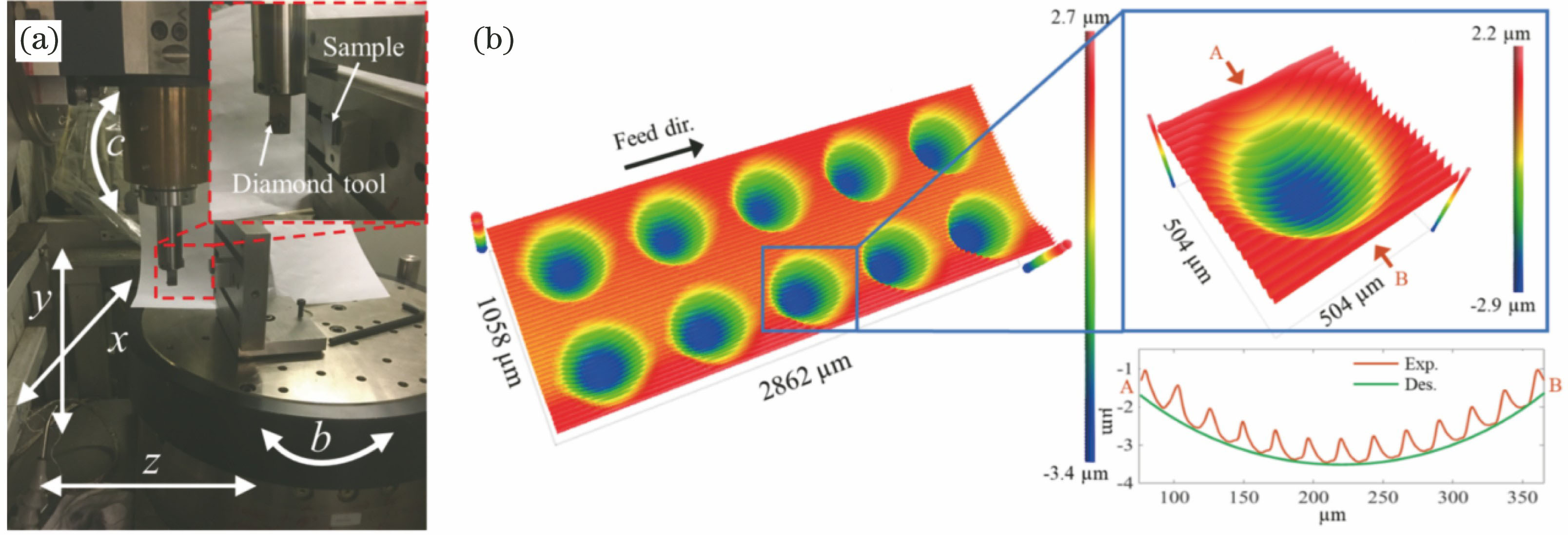
![Fabrication of IR microlens array on Si substrate by ultra-precision milling method[40]. (a) Micro-milling system with diamond tool; (b) surface morphology of the machined microlens array](/richHtml/lop/2020/57/7/071607/img_1.jpg)
Fig. 1. Fabrication of IR microlens array on Si substrate by ultra-precision milling method[40]. (a) Micro-milling system with diamond tool; (b) surface morphology of the machined microlens array
![Si microlens/micromirror array coupling device[44]. (a) Design and integration scheme of the coupling array structure; (b) SEM image of cross-section of micromirror array; (c) SEM image of microlens array; (d) focused light spots image with the coupling device; (e) single light spot image](/richHtml/lop/2020/57/7/071607/img_2.jpg)
Fig. 2. Si microlens/micromirror array coupling device[44]. (a) Design and integration scheme of the coupling array structure; (b) SEM image of cross-section of micromirror array; (c) SEM image of microlens array; (d) focused light spots image with the coupling device; (e) single light spot image
Fig. 3. Schematic diagram of Si microlens fabrication by femtosecond laser assisted wet etching[56]
Fig. 4. SEM images of evolution of micro concave surface morphology with wet etching time[56]. (a) 1 min; (b) 5 min; (c) 10 min
Fig. 5. SEM images of Si microlens array by femtosecond laser assisted wet etching[59]. (a) Hexagonal microlens array; (b) zoomed image of the hexagonal microlens array; (c) rectangular microlens array; (d) zoomed image of the rectangular microlens array
Fig. 6. Measurement of reflective foci through the Si microlens array[59]. (a) Schematic of the optical measurement setup; (b) focal spots image of the rectangular microlens array; (c) focal spots image of the hexagonal microlens array; (d) intensity distribution of the foci array through the rectangular microlens array
Fig. 7. Quasi-periodic Si microlens array by femtosecond laser assisted wet etching and its reflective beam homogenizing effect[60]. (a) SEM image of the quasi-periodic Si microlens array; (b) 3D morphology of the microlens array; (c) optical system used for measuring the homogenized illumination; (d) far field homogenized illumination with Si microlens array reflection; (e) far field illumination distribution with polished Si substrate reflection; (f) 3
Fig. 8. Profilometer image of As2Se3 thin film microlens array[45]. (a) Optical image of the convex microlens arrays, the inset shows the grayscale mask used; (b) 3D view of the convex microlens arrays; (c) optical image of the concave microlens arrays, the inset shows the grayscale mask used; (d) 3D view of the concave microlens arrays
Fig. 9. Fabrication and application of As2S3 infrared microlens array by heated compression molding[41]. (a) Schematic diagrams of the compression molding process and the fabricated infrared microlens array; (b) schematic of the S-H wavefront sensor by the prepared microlens array sample; (c) measured image and lattice diagram image
Fig. 10. Chalcogenide glass IR microlens array by femtosecond laser direct writing method, its virtual focal spots, and virtual images of the letters “P” [68]
Fig. 11. Tunable microlens array component based on IR liquid crystal[70]. (a) Schematic of the IR liquid crystal microlens array; (b) appearance of the fabricated component; (c) experimental setup for measuring the optical properties of the fabricated component; (d) IR microbeam convergence by single microlens
Fig. 12. Planar IR polymer microlens array component[51]. (a) Macro 3D morphology of the fabricated component; (b) SEM image of the surface morphology of the IR microlens array; (c) measured transverse profile of the microlenslets; (d) measured MTF of the imaging unit
Fig. 13. NIR images of a tungsten lamp sampled by the fabricated microlens array component[51]. (a) Active IR image with environment illumination (10×); (b) passive IR image with object luminescence (10×); (c) active IR image with environment illumination (20×); (d) passive IR image with object luminescence (20×)
Fig. 14. Planar IR microlens array used in the parallel micro-inscription[51]. (a) Laser induced surface damage threshold measurement by the laser ablation probability; (b) parallel laser micro-inscription pattern on the polymer target by the planar IR microlens array device
Fig. 15. 3D IR compound eye component[52]. (a) Macro morphology of the fabricated component; (b) surface morphology of the fabricated component; (c) focal length and the numerical aperture of the micro-lenslets along the radial direction; (d) transmittance of the fabricated component
Fig. 16. IR imaging with the IR compound eye component[52]. (a) Imaging of the USAF1951 resolution test chart through single ommatidium; (b) active IR imaging of the flame pattern target through compound eye; (c) passive IR imaging of a heated nichrome wire target (5×); (d) zoomed passive IR image of the heated nichrome wire target (20×); (e) IR image of the direction indicator target with central part in focus; (f) IR image of the direction indicator tar

Set citation alerts for the article
Please enter your email address


