Abstract
Thin-film lithium niobate is a promising material platform for integrated nonlinear photonics, due to its high refractive index contrast with the excellent optical properties. However, the high refractive index contrast and correspondingly small mode field diameter limit the attainable coupling between the waveguide and fiber. In second harmonic generation processes, lack of efficient fiber-chip coupling schemes covering both the fundamental and second harmonic wavelengths has greatly limited the overall efficiency. We design and fabricate an ultra-broadband tri-layer edge coupler with a high coupling efficiency. The coupler allows efficient coupling of 1 dB / facet at 1550 nm and 3 dB / facet at 775 nm. This enables us to achieve an ultrahigh overall second harmonic generation normalized efficiency (fiber-to-fiber) of 1027 % W - 1 cm - 2 (on-chip second harmonic efficiency ∼3256 % W - 1 cm - 2) in a 5-mm-long periodically-poled lithium niobate waveguide, which is two to three orders of magnitude higher than that in state-of-the-art devices.
Video Introduction to the Article
1 Introduction
Lithium niobate is an ideal material for nonlinear photonics due to its exceptional nonlinear-optic properties, wide transparency range, and ferroelectric properties.1,2 Periodically poled lithium niobate (PPLN) waveguides, where the periodic domain inversion allows for a quasi-phase-matched (QPM) second-order nonlinear [] process, have been widely used in wavelength conversion,3,4 optical parametric oscillation,5–8 photon pair generation,9–12 and supercontinuum generation.13–15 As the strength of the nonlinear interaction is proportional to the optical intensity, the employment of high-contrast waveguides with strong optical confinement can greatly improve nonlinear optical efficiency. Unfortunately, the legacy PPLN waveguides are based on weakly confined waveguides with index contrasts of , leading to low nonlinear interaction strengths. Therefore, the traditional PPLN device requires a long interaction length for high conversion efficiency, making it difficult for large-scale photonic integrated circuits. In recent years, thin-film lithium niobate (TFLN) has emerged as an attractive platform for compact and high-performance optical modulators16–18 and nonlinear optical devices19–24 due to the high refractive index contrast () offered by TFLN waveguides. TFLN-based PPLN devices have been demonstrated that outperform their legacy counterparts in both nonlinear optical efficiency and device footprint.25–28 For instance, the efficiency of second harmonic generation (SHG) has been improved over 20 times in TFLN-based PPLN devices.26 However, TFLN-based PPLN devices face a major challenge of how to achieve efficient and broadband off-chip coupling. For example, in Ref. 29 an on-chip SHG conversion efficiency as high as was achieved in a 5-mm PPLN waveguide, but the collected second harmonic () power is only several when the input pump () power is nearly about 100 mW due to the lack of a well-designed coupling mechanism. For SHG, an ideal device requires an efficient coupling scheme for both the near-infrared () and near-visible () bands. Recently, several off-chip coupling schemes based on an edge coupler have been demonstrated for efficient coupling at 1550 nm.30–32 Nonetheless, an efficient edge coupler that can cover both near-infrared () and near-visible () has not been reported yet.
In this paper, we propose and demonstrate an efficient and ultra-broadband edge coupler in an x-cut TFLN platform for the fundamental transverse electric () mode by employing a low-index waveguide and a tri-layer TFLN waveguide taper structure. The measured off-chip coupling loss for 1550 and 775 nm is 1 and , respectively. In addition, we demonstrate a highly efficient SHG in a TFLN-based PPLN waveguide with this ultra-broadband edge coupler, exhibiting an ultra-high overall SHG normalized efficiency of and a corresponding on-chip efficiency of , respectively.
2 Design and Simulation
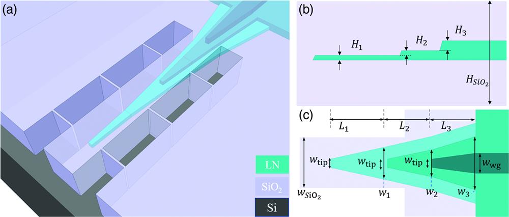
The proposed edge coupler is based on an x-cut TFLN platform (from NANOLN) with 360-nm lithium niobate and on silicon (Si) substrate. As illustrated schematically in Fig. 1(a), the coupler consists of a suspended waveguide, and a tri-layer spot size converter (SSC) including top-, middle-, and bottom-layer tapers. The light from lensed fiber is first coupled into waveguide, and then transferred to the TFLN rib waveguides through the SSC. The TFLN rib waveguides have a top width of , a slab thickness of 180 nm, and a rib height of 180 nm. A cross sectional view of the coupler is depicted in Fig. 1(b), where , , and represent the thickness of the bottom-, middle-, and top-layer of the SSC, respectively. Figure 1(c) shows the top-view of the SSC, in which , (, 2, 3), and denote the lengths, widths, and tip width of tapers. We note here that the is usually larger than 80 nm, which is limited by the fabrication process.
Sign up for Advanced Photonics Nexus TOC. Get the latest issue of Advanced Photonics Nexus delivered right to you!Sign up now

Figure 1.(a) Three-dimensional structure schematic diagram of the coupler; (b) cross-sectional view and (c) top view of coupler.
We select 1550 and 775 nm as the target wavelengths for designing the waveguide and the TFLN SSC. First, we calculate the mode overlap between the waveguide and lensed fiber to optimize the size of the waveguide. The mode field diameters of lensed single-mode optical fibers are set to be at 1550 nm and at 775 nm, respectively. As shown in Fig. 2(a), the size of the waveguide is set to be to ensure a mode overlap efficiency of for both wavelengths. Secondly, we carefully designed the SSC, especially the thickness and the tip-width of the bottom layer, to achieve adiabatic mode transition from waveguide to the TFLN rib waveguide. We calculated the coupling loss between the waveguide and LN bottom layer as functions of the tip-width at both 775 nm [Fig. 2(b)] and 1550 nm [Fig. 2(c)]. These results are obtained by eigenmode expansion (EME) method by setting a sufficiently long length of LN bottom taper. In Fig. 2(b), for a thickness , the coupling loss between the waveguide and LN bottom layer is more than 2 dB at 775 nm if the tip-width is larger than 80 nm. This reveals that a double layer SSC with a bottom layer thicknesses of 180 nm cannot achieve an efficient coupling for 775-nm light. Thus, we adopt a TFLN SSC with tri-layer structure. The tip width of the tri-layer structure is 100 nm, and the thicknesses of bottom-, middle-, and top-layer are set as 90, 90, and 180 nm, respectively. With this bottom tip size, the minimum coupling loss from the waveguide to the LN bottom layer can be at both wavelengths. Additionally, we simulated the lengths of the SSC by EME solver. As shown in Figs. 2(d)–2(f), the taper lengths were designed to be , , and to allow a sufficient mode transfer. All the other parameters of the SSC are given in Table 1.
Figure 2.(a) The simulated overlap between the lensed fiber mode and the waveguide mode at 1550 and 775 nm under different waveguide widths. Coupling loss from the waveguide to the LN bottom layer at (b) 775 nm and (c) 1550 nm with different bottom dimensions (inset: dimensional parameters of the bottom cone). The simulated curves of coupling lengths (d) , (e) , and (f) at 1550 and 775 nm. The red stars represent the designed parameter values of the coupler.
| Parameter | Value () | Parameter | Value () | Parameter | Value () |
| MFD for 1550 nm/775 nm | 3.5/2.5 | | 0.18 | | 1.2 |
| 4 | | 0.1 | | 200 |
| 4 | | 1.5 | | 100 |
| 0.09 | | 1.5 | | 100 |
| 0.09 | | 4 | — | — |
Table 1. Parameters of the designed coupler.
Figure 3(a) shows the transverse electric () mode field distribution of 1550 and 775 nm at different cross-sections of the designed edge coupler. We can see that the mode fields of both wavelengths are first well-confined in the waveguide [labeled I in Fig. 3(a)]. Subsequently, the 775- and 1550-nm wavelength light is coupled to the TFLN rib waveguide via the bottom-, middle-, and top-layer of SSC. Figures 3(b) and 3(c) show the snapshot of the mode evolution process at both wavelengths. A simulated coupling loss of at 1550 nm and at 775 nm is obtained for mode after optimization, while that for the transverse magnetic () mode is more than 3 and at the two wavelengths, showing a polarization dependence of the designed coupler. This is advantageous for nonlinear frequency conversion based on x-cut TFLN platform, where the mode is usually used to exploit the maximum nonlinear coefficient of lithium niobate.
Figure 3.(a) The simulated distribution of mode of 1550 and 775 nm at different cross sections I, II, III, IV, and V; simulated mode propagation in the designed coupler at wavelengths (b) 1550 nm and (c) 775 nm.
For comparison, we calculated the coupling efficiencies of the proposed edge coupler with tri-layer SSC and the traditional coupler with double layer SSC, respectively. As illustrated in Figs. 4(a) and 4(b), these simulated results clearly show that the present edge coupler with tri-layer SSC (the solid curves) features ultra-broadband operation covering both 1550- and 775-nm bands, while the edge coupler with double layer SSC (the dotted curves) only works well in the 1550-nm band.
Figure 4.The simulated coupling efficiency of double-layer structure and tri-layer structure at (a) 1550- and (b) 775-nm band.
3 Fabrication
The device fabrication process is as follows. First, the rib waveguides and the top layer of SSC are defined with HSQ resist by electron-beam lithography (EBL), and transferred to TFLN by using Ar ion in inductively coupled plasma (ICP) system. The etching depth of waveguide is 180 nm. Then, the middle- and bottom-layers of the SCC are prepared by EBL, photolithography, and ICP etching. Figures 5(a), 5(b), and 5(c) show the scanning electron microscope (SEM) pictures of the tips of the bottom-, middle-, and top-layer, respectively. After the fabrication of the SSC, a -thick is deposited by plasma-enhanced chemical vapor deposition. The waveguides with supporting arms are patterned by photolithography and etched by chemistry. Finally, the underlying silicon substrate is removed by two-step etching processes. An isotropic etching with is first utilized to suspend the waveguide, while a Bosch deep silicon anisotropic dry etch process with is used to expose the coupling interface between optical fiber and chip. A smooth sidewall and coupling interface are observed in the SEM pictures in Figs. 5(d) and 5(e).
Figure 5.SEM pictures of (a) bottom tip, (b) middle tip, and (c) top tip. (d) SEM picture and (e) larger view of suspended waveguide.
4 Results and discussions
4.1 Coupling Efficiency Characterization
The coupling efficiency of the edge coupler is characterized by several 5-mm-long reference waveguides. The propagation losses of the waveguides are at 1550 nm and at 775 nm. Two lensed fibers and a fiber polarization controller (FPC) are applied for mode coupling. We measured the coupling transmission spectra at near-infrared band (1535 to 1565 nm) and near-visible band (765 to 780 nm). Figures 6(a) and 6(b) show the mean values of coupling losses for the mode and its standard deviation over six devices on the same wafer. The mean coupling losses are at 1550 nm and at 775 nm, respectively. The measured results show lower coupling efficiency than the simulated one, which is predominately originated from the scattering losses of the multi-layer structure and propagation loss of waveguide with supporting arm which are estimated to less than 0.5 dB at 1550 nm and 0.25 dB at 775 nm according to 3D FDTD simulation.
Figure 6.The coupling losses of the fabricated edge couplers at (a) 1535 to 1565 nm and (b) 765 to 780 nm. Shadowed areas show the standard deviation measured over six devices.
4.2 Second Harmonic Generation
We also fabricate 5-mm-long PPLN waveguides along with designed edge coupler for SHG. The width and thickness of the PPLN waveguide is designed as and 180 nm. According to the QPM condition , we obtained the poling period for type-0 scheme by simulating the mode effective indexes at second harmonic () and pump () wavelength. Taking fabrication error into consideration, several PPLN waveguides with poling periods ranging from 3.10 to in 10-nm steps are prepared in experiment. The periodic poling process can be divided into two steps.21 First, the comb-shaped electrodes consisting of 30-nm NiCr and 40-nm Au were deposited on the x-cut TFLN before the fabrication of waveguide. Then several high-voltage pulses about 300 V were applied, and the period domains were checked via SHG imaging technique using confocal microscope to optimize the pulse duration time and the number of pulses. Figure 7(a) shows the period domain observed by SHG-confocal microscope imaging, which shows the domain-inverted region with duty cycle close to 50:50 (red frame).
Figure 7.(a) Period domain observed by SHG-confocal microscope imaging; red frame is the domain-inverted region. (b) Experimental setup for SHG. FPC, fiber polarization controller; OSA, optical spectrum analyzer. (c) Measured normalized SHG conversion efficiency versus pump wavelengths. (d) Quadratic power dependence of the SH wave on the pump wave.
The experimental setup for SHG is shown in Fig. 7(b). The pump light from a C-band tunable laser is adjusted to via an FPC, and subsequently coupled from the lensed fiber into the PPLN waveguide utilizing the edge coupler. The generated second harmonic signal is coupled out from the chip by a second lensed fiber and finally monitored with a Si photodiode power sensor or an optical spectrum analyzer (OSA). We first investigate the SHG spectral profile of the PPLN waveguide by scanning the pump wavelength. As depicted in Fig. 7(c), the main QPM peak is centered at 1563.1 nm with a full width at half-maximum bandwidth of 1.5 nm. By fixing the pump wavelength at 1563.1 nm and gradually increasing the pump power, we obtain the quadratic power dependence of the second harmonic wave on the pump light [see Fig. 7(d)] and a slope of is extracted by linearly fitting the experimental data. The normalized efficiency is calculated to be , which is 70% of the theoretical efficiency ().33 The lower maximum efficiency is mainly caused by the inhomogeneity of the thin-film thickness over the 5-mm waveguide length.34,35 We define an overall normalized efficiency by dividing the collected second harmonic power by the square of the input pump light and the square of the poled waveguide length. By taking account of the off-chip coupling efficiency (1 dB per facet) at 1563.1 nm and (3 dB per facet) at 781.55 nm, the overall normalized efficiency is counted to be according to formula of .
5 Conclusions
We implement an edge coupler featuring low coupling loss and ultra-broad bandwidth. The off-chip efficiency at 755 and 1550 nm is 3 and , respectively. The experimental coupling efficiency of the coupler in the near-visible light band is 3 dB higher than the simulated efficiency of the traditional two-layer structure. Based on this designed coupling scheme, we acquire an ultrahigh overall SHG normalized efficiency of in a 5-mm-long PPLN waveguide, corresponding to a high on-chip SHG normalized efficiency of . Compared with the state-of-the-art (Table 2), the overall conversion efficiency of the present PPLN devices is increased by two to three orders of magnitude, benefitting from the improvement of coupling efficiency at the pump light and second harmonic wave. This high-efficiency and ultra-broadband edge coupler greatly reduces the power consumption in the process of nonlinear frequency conversion, showcasing obvious advantages in practical nonlinear applications.
| Ref. | Length (mm) | (% ) | (% ) | Pump/SH coupling loss (dB/facet) |
| 21 | 6 | 3061 | 3a | 10/10 |
| 24 | 0.6 | 4600 | 57.5a | 6/7 |
| 26 | 4 | 2600 | 2.6a | 10/10 |
| 29 | 5 | 3757 | 9.65a | 6.7/12.5 |
| This work | 5 | 3256 | 1027 | 1/3 |
Table 2. A comparison with other SHG works based on periodically poled TFLN waveguides.
Biographies of the authors are not available.
References
[1] V. Gopalan et al. Defect-domain wall interactions in trigonal ferroelectrics. Annu. Rev. Mater. Res., 37, 449-489(2007).
[2] R. S. Weis et al. Lithium niobate: summary of physical properties and crystal structure. Appl. Phys. A, 37, 191-203(1985).
[3] J. Zhang et al. Flexible wavelength conversion via cascaded second order nonlinearity using broadband SHG in MgO-doped PPLN. Opt. Express, 16, 6957-6962(2008).
[4] M. Gong et al. All optical wavelength broadcast based on simultaneous type I QPM broadband SFG and SHG in MgO:PPLN. Opt. Lett., 35, 2672-2674(2010).
[5] A. V. Okishev et al. Intracavity-pumped Raman laser action in a mid-IR, continuous-wave (CW) MgO:PPLN optical parametric oscillator. Opt. Express, 14, 12169-12173(2006).
[6] I.-H. Bae et al. Low-threshold singly-resonant continuous-wave optical parametric oscillator based on MgO-doped PPLN. Appl. Phys. B, 103, 311-319(2011).
[7] T. Wang et al. Electro-optically spectrum switchable, multiwavelength optical parametric oscillators based on aperiodically poled lithium niobate. Opt. Lett., 45, 5848-5851(2020).
[8] J. Lu et al. Ultralow-threshold thin-film lithium niobate optical parametric oscillator. Optica, 8, 539-544(2021).
[9] S. Tanzilli et al. PPLN waveguide for quantum communication. Eur. Phys. J. D, 18, 155-160(2002).
[10] X. Lu et al. Chip-integrated visible–telecom entangled photon pair source for quantum communication. Nature Physics, 15, 373-381(2019).
[11] B. S. Elkus et al. Generation of broadband correlated photon-pairs in short thin-film lithium-niobate waveguides. Opt. Express, 27, 38521-38531(2019).
[12] J. Zhao et al. High quality entangled photon pair generation in periodically poled thin-film lithium niobate waveguides. Phys. Rev. Lett., 124, 163603(2020).
[13] C. R. Phillips et al. Supercontinuum generation in quasi-phase-matched LiNbO3 waveguide pumped by a Tm-doped fiber laser system. Opt. Lett., 36, 3912-3914(2011). https://doi.org/10.1364/OL.36.003912
[14] M. Yu et al. Coherent two-octave-spanning supercontinuum generation in lithium-niobate waveguides. Opt. Lett., 44, 1222-1225(2019).
[15] J. Lu et al. Octave-spanning supercontinuum generation in nanoscale lithium niobate waveguides. Opt. Lett., 44, 1492-1495(2019).
[16] C. Wang et al. Nanophotonic lithium niobate electro-optic modulators. Opt. Express, 26, 1547-1555(2018).
[17] C. Wang et al. Monolithic lithium niobate photonic circuits for Kerr frequency comb generation and modulation. Nat. Commun., 10, 978(2019).
[18] M. He et al. High-performance hybrid silicon and lithium niobate Mach–Zehnder modulators for 100 Gbit s−1 and beyond. Nat. Photonics, 13, 359-364(2019).
[19] M. Xu et al. High-performance coherent optical modulators based on thin-film lithium niobate platform. Nat. Commun., 11, 3911(2020).
[20] J. -Y. Chen et al. Ultra-efficient frequency conversion in quasi-phase-matched lithium niobate microrings. Optica, 6, 1244-1245(2019).
[21] Y. Niu et al. Optimizing the efficiency of a periodically poled LNOI waveguide using in situ monitoring of the ferroelectric domains. Appl. Phys. Lett., 116, 101104(2020).
[22] J. Lu et al. Periodically poled thin-film lithium niobite microring resonators with a second-harmonic generation efficiency of 250,000%/W. Optica, 6, 1455-1460(2019).
[23] G. -T. Xue et al. “Ultrabright multiplexed energy-time-entangled photon generation from lithium niobate on insulator chip. “Phys. Rev. Appl, 15, 064059(2021).
[24] A. Rao et al. Actively-monitored periodic-poling in thin-film lithium niobate photonic waveguides with ultrahigh nonlinear conversion efficiency of 4600 % W−1cm−2. Opt. Express, 27, 25920-25930(2019). https://doi.org/10.1364/OE.27.025920
[25] D. Zhu et al. Integrated photonics on thin-film lithium niobate. Adv. Opt. Photonics, 13, 242-352(2021).
[26] C. Wang et al. Ultrahigh-efficiency wavelength conversion in nanophotonic periodically poled lithium niobate waveguides. Optica, 5, 1438-1441(2018).
[27] X. Liu et al. Highly efficient thermo-optic tunable micro-ring resonator based on an LNOI platform. Opt. Lett., 45, 6318-6321(2020).
[28] R. Gao et al. Lithium niobate microring with ultra-high Q factor above 108. Chin. Opt. Lett., 20, 011902(2022).
[29] J. Zhao et al. Shallow-etched thin-film lithium niobate waveguides for highly-efficient second-harmonic generation. Opt. Express, 28, 19669-19682(2020).
[30] L. He et al. Low-loss fiber-to-chip interface for lithium niobate photonic integrated circuits. Opt. Lett., 44, 2314-2317(2019).
[31] C. Hu et al. High-efficient coupler for thin-film lithium niobate waveguide devices. Opt. Express, 29, 5397-5406(2021).
[32] Y. Pan et al. Low-loss edge-coupling thin-film lithium niobate modulator with an efficient phase shifter. Opt. Lett., 46, 1478-1481(2021).
[33] L. Chang et al. Thin film wavelength converters for photonic integrated circuits. Optica, 3, 531-535(2016).
[34] X.-H. Tian et al. Effect of dimension variation for second-harmonic generation in lithium niobate on insulator waveguide. Chin. Opt. Lett., 19, 060015(2021).
[35] M. Santandrea et al. Characterisation of fabrication inhomogeneities in Ti:LiNbO3 waveguides. New J. Phys., 21, 123005(2019). https://doi.org/10.1088/1367-2630/ab5cb5