• Journal of Infrared and Millimeter Waves
  • Vol. 41, Issue 2, 395 (2022)
Jia-Hua TAO1 and Jun-Hao CHU1、2、*
Author Affiliations
  • 1Nanophotonics and Advanced Instrument Engineering Research Center,Ministry of Education,Key Laboratory of Polar Materials and Devices,Ministry of Education,East China Normal University,Shanghai 200241,China
  • 2National Laboratory for Infrared Physics,Shanghai Institute of Technical Physics,Chinese Academy of Sciences,Shanghai,200083,China
  • show less
    DOI: 10.11972/j.issn.1001-9014.2022.02.004 Cite this Article
    Jia-Hua TAO, Jun-Hao CHU. Research progress and challenges of copper indium gallium selenide thin film solar cells[J]. Journal of Infrared and Millimeter Waves, 2022, 41(2): 395 Copy Citation Text show less
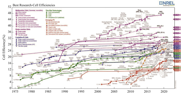
    Best laboratory certified efficiencies for CIGS solar cells [19]
    Fig. 1. Best laboratory certified efficiencies for CIGS solar cells 19
    (a,b)Schematics of the device structure of the small-area cell and the monolithically-connected module structure,respectively.(c)Schematics of the typical band profile in the CIGS absorber layer. EC and EV represent the energetic positions of the conduction band minimum and the valence band maximum,respectively. Front and back correspond to the buffer/CIGS and the CIGS/Mo interfaces,respectively[20]
    Fig. 2. (a,b)Schematics of the device structure of the small-area cell and the monolithically-connected module structure,respectively.(c)Schematics of the typical band profile in the CIGS absorber layer. EC and EV represent the energetic positions of the conduction band minimum and the valence band maximum,respectively. Front and back correspond to the buffer/CIGS and the CIGS/Mo interfaces,respectively20
    Schematic illustration of different co-evaporation processes:(a)single stage process,(b)bilayer or Boeing process in which the first layer was deposited at lower substrate temperature, and the second layer was deposited at a higher substrate temperature,(c)three stage process in which In and Ga are deposited in the first and third stage, whereas Cu was deposited in the second stage(after Ref. [33])
    Fig. 3. Schematic illustration of different co-evaporation processes:(a)single stage process,(b)bilayer or Boeing process in which the first layer was deposited at lower substrate temperature, and the second layer was deposited at a higher substrate temperature,(c)three stage process in which In and Ga are deposited in the first and third stage, whereas Cu was deposited in the second stage(after Ref. [33])
    Fabrication process of Solar Frontier’s baseline CIGS solar cell [20]
    Fig. 4. Fabrication process of Solar Frontier’s baseline CIGS solar cell [20]
    (a)Schematics of the profiles of composition and bandgap in the CIGS absorber layer to explain the condition of the device simulation.(b)Device simulation results with varying surface [S]/([S]+[Se])composition and position of the bandgap minimum(xEg,min)(after Ref. [20])
    Fig. 5. (a)Schematics of the profiles of composition and bandgap in the CIGS absorber layer to explain the condition of the device simulation.(b)Device simulation results with varying surface [S]/([S]+[Se])composition and position of the bandgap minimum(xEg,min)(after Ref. [20])
    After Na incorporation into the CIGS film,the following changes were observed:(a)enhanced carrier density and grain boundary passivation,(b)gallium segregation,and(c)changes in crystallographic orientation(after Ref.[45])
    Fig. 7. After Na incorporation into the CIGS film,the following changes were observed:(a)enhanced carrier density and grain boundary passivation,(b)gallium segregation,and(c)changes in crystallographic orientation(after Ref.[45])
    Surface chemical analysis(a)Schematic view of the three investigated absorbers. The purple layer on the KF absorber indicates the modified surface composition,(b-e)XPS peak of Cu 2p3/2,In 3d5/2,Ga 2p3/2 and Se 3s,respectively,obtained from the surface of CIGS absorbers with no alkali evaporation(no PDT),only NaF addition and only KF addition,(f)Sputtering of the CIGS absorber subjected to KF-PDT shows the appearance of the Cu 2p3/2 peak within the first approximately 20 nm with similar intensity as in the case of no PDT,(g)K is clearly measurable at the surface up to a depth of approximately 20 nm,(h)Schematic view of two absorbers measured after sputtering through the CdS layer,(i)XPS peak of Cu 2p3/2,In 3d5/2,Ga 2p3/2 and Se 3s,respectively,at the CdS/CIGS interface with only NaF addition and only KF addition,(m)XPS spectra of K at different sputtering depths(after Ref.[48])
    Fig. 8. Surface chemical analysis(a)Schematic view of the three investigated absorbers. The purple layer on the KF absorber indicates the modified surface composition,(b-e)XPS peak of Cu 2p3/2,In 3d5/2,Ga 2p3/2 and Se 3s,respectively,obtained from the surface of CIGS absorbers with no alkali evaporation(no PDT),only NaF addition and only KF addition,(f)Sputtering of the CIGS absorber subjected to KF-PDT shows the appearance of the Cu 2p3/2 peak within the first approximately 20 nm with similar intensity as in the case of no PDT,(g)K is clearly measurable at the surface up to a depth of approximately 20 nm,(h)Schematic view of two absorbers measured after sputtering through the CdS layer,(i)XPS peak of Cu 2p3/2,In 3d5/2,Ga 2p3/2 and Se 3s,respectively,at the CdS/CIGS interface with only NaF addition and only KF addition,(m)XPS spectra of K at different sputtering depths(after Ref.[48])
    Schematic drawing of the NaF PDT and the NaF&KF PDT applied on low-temperature coevaporated CIGS thin films [49]
    Fig. 9. Schematic drawing of the NaF PDT and the NaF&KF PDT applied on low-temperature coevaporated CIGS thin films 49
    External quantum efficiency for CIGS cells with different buffer materials. All cells with anti-reflection coatings. The shaded areas below the curves represent the current gain relative to the corresponding CdS reference when available(after Ref.[53])
    Fig. 10. External quantum efficiency for CIGS cells with different buffer materials. All cells with anti-reflection coatings. The shaded areas below the curves represent the current gain relative to the corresponding CdS reference when available(after Ref.[53])
    (a)Comparison of the optical properties of AZO and BZO with comparable sheet resistance. The high transmission in the near-infrared region for BZO stems from the reduced carrier density(AZO n=4.4*1020 cm-3,BZO n=9.2*1019 cm-3)(after Ref.[64]).(b)Damp heat stability(85 °C,85% r.h.)of different,nonencapsulated TCO materials(after Ref.[70-72])
    Fig. 11. (a)Comparison of the optical properties of AZO and BZO with comparable sheet resistance. The high transmission in the near-infrared region for BZO stems from the reduced carrier density(AZO n=4.4*1020 cm-3,BZO n=9.2*1019 cm-3)(after Ref.[64]).(b)Damp heat stability(85 °C,85% r.h.)of different,nonencapsulated TCO materials(after Ref.[70-72])
    Photovoltaic application products such as flexible CIGS thin film solar cell template and building integration[73]
    Fig. 12. Photovoltaic application products such as flexible CIGS thin film solar cell template and building integration[73]
    (a)Schematic of the 4-T perovskite/CIGS tandem solar cell.(b)J-V curves of the CIGS cell with and without filtering,and reverse and forward scanning curves(scanning rate of 50 mV s-1)and steady-state efficiency of the semi-transparent perovskite.(c)Transmittance and absorption spectra and EQE of the transparent perovskite cells,and EQE of the standalone CIGS and that placed under a filter(after Ref.[89])
    Fig. 13. (a)Schematic of the 4-T perovskite/CIGS tandem solar cell.(b)J-V curves of the CIGS cell with and without filtering,and reverse and forward scanning curves(scanning rate of 50 mV s-1)and steady-state efficiency of the semi-transparent perovskite.(c)Transmittance and absorption spectra and EQE of the transparent perovskite cells,and EQE of the standalone CIGS and that placed under a filter(after Ref.[89])
    Performance of the perovskite/CIGS tandem cells.(a)Schematic and cross-sectional SEM image of the monolithic perovskite/CIGS tandem solar cell.(b)J-V curve and efficiency at the maximum power point(inset)of the champion tandem device.(c)EQE spectra for the subcells of the monolithic perovskite/CIGS tandem solar cell.(d)Stability test of the monolithic perovskite/CIGS tandem solar cell. The unencapsulation device maintained 88% of their initial PCE after 500 hours of aging under continuous 1-sun illumination and maximum power point tracking at 30 °C ambient environment. The inset shows that the device can recover 93% of its initial performance after a 12-hour resting period without load and illumination(after Ref.[90])
    Fig. 14. Performance of the perovskite/CIGS tandem cells.(a)Schematic and cross-sectional SEM image of the monolithic perovskite/CIGS tandem solar cell.(b)J-V curve and efficiency at the maximum power point(inset)of the champion tandem device.(c)EQE spectra for the subcells of the monolithic perovskite/CIGS tandem solar cell.(d)Stability test of the monolithic perovskite/CIGS tandem solar cell. The unencapsulation device maintained 88% of their initial PCE after 500 hours of aging under continuous 1-sun illumination and maximum power point tracking at 30 °C ambient environment. The inset shows that the device can recover 93% of its initial performance after a 12-hour resting period without load and illumination(after Ref.[90])
    方法优点缺点
    共蒸发对于实验室小电池是一种良好的制备技术同时控制不同蒸发源是困难和化学计量变化大,重现性低和大面积均匀性差
    磁控溅射较好地控制沉积速度和获得较好结晶性,有利于工业化生产运行成本较高,容易产生多相,带隙梯度调控困难
    电沉积低成本、室温沉积工艺优化困难
    丝网印刷术材料损耗低,堆积密度大,高产能在喷涂过程中原材料损耗大
    旋涂法实验室制备薄膜均匀性,设备成本低,操作方便大面积不均匀,卷对卷工艺不兼容
    刮涂法材料浪费少,卷对卷工艺兼容,更好的化学计量控制溶剂蒸发速度慢,容易堆积
    分子束外延超高真空沉积造成污染最小,该方法有利于基础研究,如缺陷和相分离研究不适合工业化生产,大面积沉积尚未报道,高效率尚未报道
    气相外延生长对基础研究有用,生长速度比分子束外延快不适合工业化生产,大面积器件未报道,工业化生产不兼容
    电子束沉积良好的化学计量比和高纯相薄膜大面积沉积未见报道,工业生产不兼容
    脉冲激光淀积靶材组分可以直接转移到薄膜上,可产良率的化学计量,可以避免CuSe二元相不适合大面积应用,大面积薄膜尚未见报道
    喷墨印刷简化了工艺生产步骤,卷对卷技术兼容低转换效率
    Table 1. List of various growth methods used for the preparation of CIGS films, and their advantages and disadvantages
    NaF PDT /minKF PDT /minGGICGIEff./(%)Voc/ mV

    Jsc

    (mA/cm2

    FF/(%)
    000.340.7912.054134.963.6
    2000.350.8213.262434.561.5
    2050.350.7917.567334.774.9
    20200.360.8018.569535.076.0
    Table 2. The influence of different alkali metal combinations on the photovoltaic parameters of CIGS solar cells
    缓冲层沉积方法窗口层Eff. /(%)Voc /V

    Jsc /

    (mA/cm-2

    FF/(%)Area /cm2研发机构参考文献
    Zn(O,S,OH)x/Zn0.8Mg0.2OCBD/ALDZnO:B23.350.73439.680.41SF18
    CdSCBDi-ZnO/ZnO:B22.90.74438.7779.51.041SF44
    Zn(O,S,OH)CBD(Zn,Mg)O/ZnO:B22.80.71141.477.5900SF54
    CdSCBDi-ZnO/ZnO:Al22.60.74137.880.60.25ZSW47
    CdSCBDi-ZnO/ZnO:Al21.70.74636.69.30.5ZSW55
    Zn(O,S)CBDZn0.75Mg0.25O/ZnO:Al21.00.71737.278.60.5Solibro56
    Zn(O,S)ALDi-ZnO/ZnO:B19.80.71536.575.80.522SF57
    Zn(O,S)SputteringZnO:Al18.30.65438.472.80.49ZSW58
    InxSyEvaporationi-ZnO/ZnO:Al18.20.67336.374.50.5ZSW59
    Zn1-xSnxOyALDi-ZnO/ZnO:Al18.20.68935.175.30.49Uppsala60
    Zn1-xMgxOALDi-ZnO/ZnO:Al18.10.66835.775.70.5Uppsala61
    ZnS(O,OH)CBDi-ZnO/ZnO:B17.90.6638.171.1900Sams62
    Zn1-xMgxOALDi-ZnO/In2O3:Sn15.50.9223.472.20.433SF63
    Table 3. Summary of best performing small-area CIGS cells with different buffer layers and respective deposition methods
    Jia-Hua TAO, Jun-Hao CHU. Research progress and challenges of copper indium gallium selenide thin film solar cells[J]. Journal of Infrared and Millimeter Waves, 2022, 41(2): 395
    Download Citation