
Xianchun Peng, Jie Sun, Huan Liu, Liang Li, Qikun Wang, Liang Wu, Wei Guo, Fanping Meng, Li Chen, Feng Huang, Jichun Ye. Structural and optical properties of AlN sputtering deposited on sapphire substrates with various orientations[J]. Journal of Semiconductors, 2022, 43(2): 022801
- Journal of Semiconductors
- Vol. 43, Issue 2, 022801 (2022)
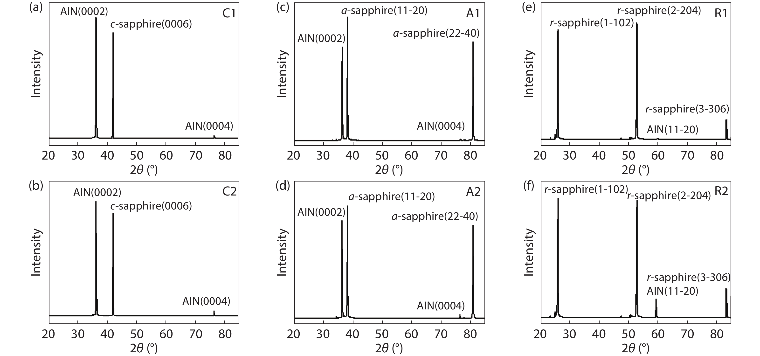
Fig. 1. Powder X-ray diffraction spectra of AlN deposited on (a, b) c , (c, d)a and (e, f) r -plane sapphire substrates before and after thermal annealing. Clear diffraction peaks from AlN and sapphire can be identified.
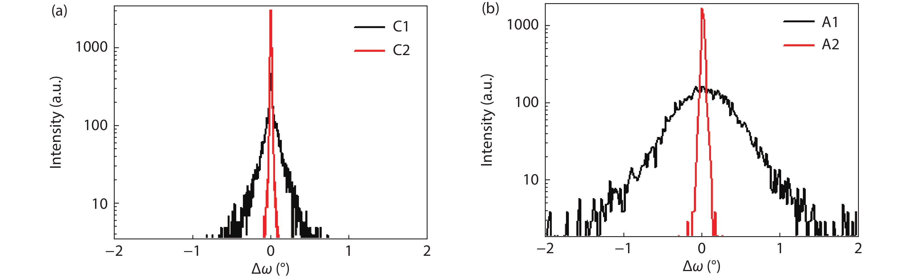
Fig. 2. (Color online) HRXRD (0002) RC scans of sputtered AlN on (a) c -plane and (b) a -plane sapphire substrates prior to and after thermal annealing.
Fig. 3. (Color online) Surface morphology of sputtered AlN on (a, b) c , (c, d) a , (e, f) r -plane sapphires prior to (a, c, e) and after (b, d, f) thermal annealing.
Fig. 4. (Color online) Optical transmission spectra and the square of absorption coefficient (α 2) versus photon energy (hν ) of sputtered AlN on (a, b) c , (c, d) a, and (e, f) r -sapphire substrates before and after thermal annealing. The band gap is derived from the intersection between the linear fitting of the absorption curve and the x axis.
Fig. 5. (Color online) Raman spectra of sputtered AlN on c, a , and r -sapphire substrates (a) prior to and (b) after HTTA. Dashed line from left to right indicatesa , r -sapphire substrates peak and strain-free Raman peak position of AlN respectively.
Fig. 6. (Color online) High-resolution XPS Al 2p core levels from samples grown on (a, b) c , (c, d) a , and (e, f) r -sapphire substrates. The core levels of Al 2p peaks are deconvoluted into Al–Al, Al–N sub-peaks before thermal annealing and Al–N, Al–O sub-peaks after thermal annealing.
| ||||||||||||||||||||||||||||||||
Table 1. Calculated absorption edges of AlN thin films acquired by α 2 versus photon energy curve, rms roughness and the FWHM of the (002) diffraction peaks.

Set citation alerts for the article
Please enter your email address
© Copyright 2018-2021 | Chinese Laser Press. All Rights Reserved 沪ICP备15018463号-20