
Xianchun Peng, Jie Sun, Huan Liu, Liang Li, Qikun Wang, Liang Wu, Wei Guo, Fanping Meng, Li Chen, Feng Huang, Jichun Ye. Structural and optical properties of AlN sputtering deposited on sapphire substrates with various orientations[J]. Journal of Semiconductors, 2022, 43(2): 022801
- Journal of Semiconductors
- Vol. 43, Issue 2, 022801 (2022)
Abstract
1. Introduction
AlN thin film is a material of great technological advantage due to its ultrawide bandgap, high breakdown voltage and strong spontaneous polarization field. Serving as a template, a variety of optoelectronic, power and RF devices are grown on top of it, including the ultraviolet light-emitting-diode (UV-LED), laser diodes and Schottky barrier diode[
Due to the lack of bulk AlN substrate with suitable size and satisfied crystalline quality, intensive efforts were paid to heteroepitaxy growth of AlN on foreign substrates including sapphire, SiC, and Si. As a result, the challenges of lattice and thermal mismatch during epitaxial growth must be taken care of. Among various epitaxial growth techniques, metal organic chemical vapor deposition (MOCVD) has been regarded as one of the most mature technologies in AlN deposition. However, epitaxial growth of AlN by MOCVD has relatively low production yield, considering the lack of a high-volume, high-temperature growth chamber. Compared with MOCVD, sputtering is an alternative technique to achieve uniform AlN thin film with size up to 6 inches at a relatively low cost[
Recently, high-temperature thermal annealing (HTTA) above 1500 °C has been acknowledged as an effective way to improve the crystallinity of AlN[
Nevertheless, despite many promising results reported on sputtered AlN thin films with HTTA, there is still a lack of comprehensive investigations on the influence of HTTA on optical properties, surface stoichiometry and strain behaviors of the sputtered AlN thin films. In addition, it is well known that sputtered AlN thin films on c-plane sapphire substrate usually exhibit +c crystal orientation. Yet non-polar and semipolar crystallographic planes are desired due to much-reduced polarization fields and consequently less influence from the quantum-confined Stark effect[
In this paper, AlN deposited on a sapphire substrate with different orientations (c, a, and r crystallographic planes) was achieved by the magnetron sputtering technique followed by HTTA. The correlations between the structural, optical, strain states as well as chemical stoichiometry of the HTTA AlN were provided. The scope of this work is to investigate the applicability of sputtered AlN grown on sapphire substrates with various orientations after HTTA, and offer design rules for the development large-size, high-performance AlN-based optoelectronic and electronic devices.
2. Experiment
AlN thin films were deposited on (0001) c-plane, non-polar (11-20) a-plane and semi-polar (10-12) r-plane 2-inch sapphire substrates via radio frequency (RF) magnetron sputtering technique. The deposition was performed in a custom-built MS450 sputter deposition system as previously reported[
The surface morphologies of the AlN thin film prior to and after HTTA were characterized by Veeco Dimension 3100V atomic force microscopy (AFM). The crystal orientation and thin film quality of AlN thin films were measured by both powder X-ray diffraction (XRD) and high-resolution X-ray diffraction (HRXRD) with an asymmetric Ge (220) monochromator. The thickness of the AlN film is measured by a J.A. Woollam M-200DI spectroscopic ellipsometer. The optical transmission spectrum of the AlN was measured by a Perkin Elmer Lambda 950 UV/Vis/NIR spectrometer equipped with an integrating sphere. Bi-axial strain conditions were characterized by a Renishaw inVia Raman spectroscopy under confocal mode. The spectrum resolution is 1 cm–1, and 532 nm green laser was used as the excitation source. Surface stoichiometry was investigated by a Kratos Axis Ultra DLD-ray photoelectron spectrometer (XPS).
3. Results and discussions
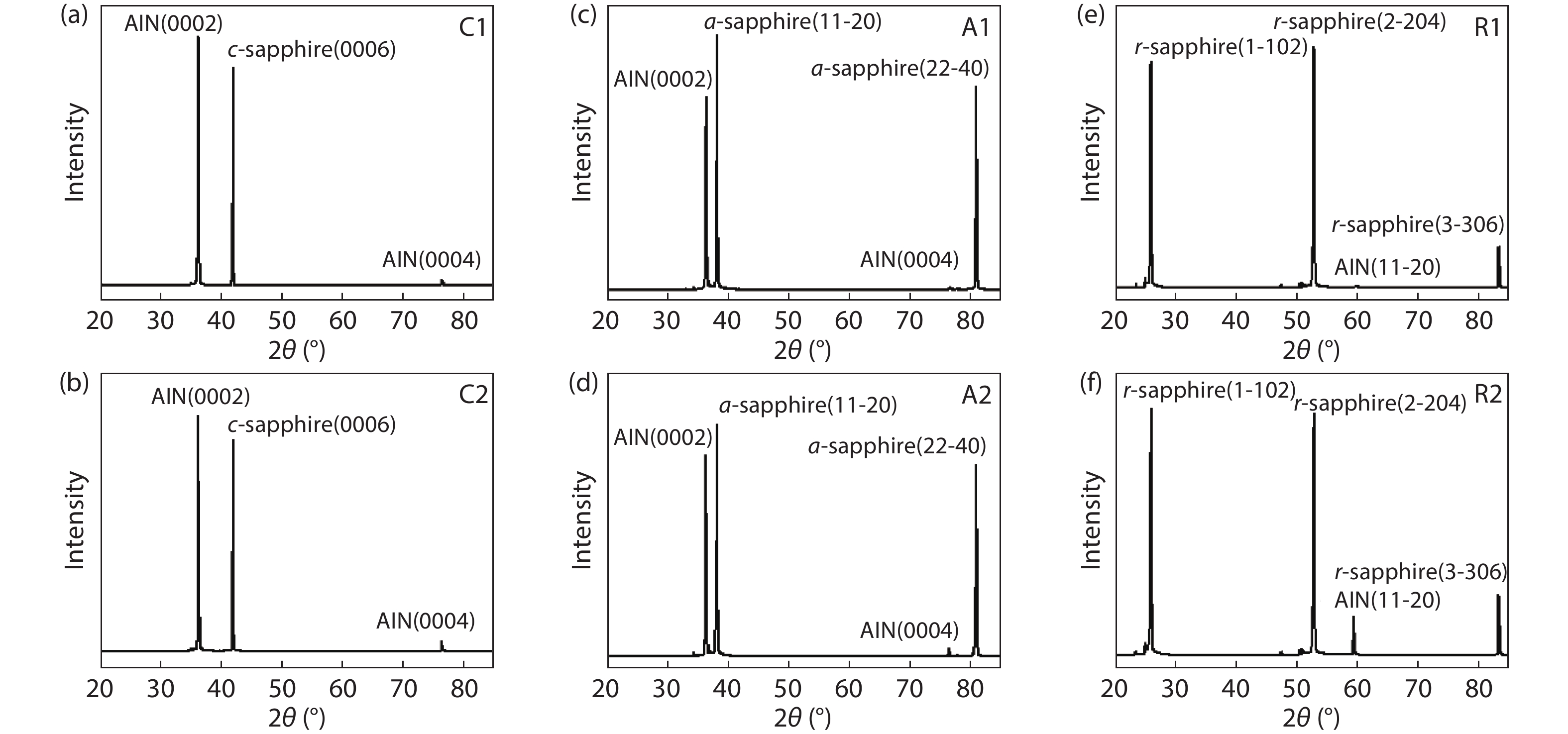
Fig. 1 shows the symmetric ω–2θ powder XRD diffractions of the AlN thin films sputter deposited on the sapphire substrates of c,a, and r-orientations with and without thermal annealing. (0002) diffraction peaks can be clearly identified from the AlN sputtered on c and a-plane sapphire substrates, indicating the successful epitaxial growth of AlN thin film. This is consistent with previous reports that c-oriented AlN is most frequently observed during sputtering[
![]()
Figure 1.Powder X-ray diffraction spectra of AlN deposited on (a, b)
To further validate the change in crystalline quality of AlN after HTTA, HRXRD rocking curve (RC) scans were employed. No significant (11-20) diffraction peak can be identified from the HRXRD scan of AlN deposited on r-sapphire possibly due to the inferior crystalline quality, thus only the results of C1/2 and A1/2 were illustrated in Fig. 2. Note that the full-width-half-maximum (FWHM) value of the (0002) RC diffraction peak is an indication of the density of screw-type dislocations, which is strongly correlated with the tilt component of the crystal grains[
![]()
Figure 2.(Color online) HRXRD (0002) RC scans of sputtered AlN on (a)
Fig. 3 shows the AFM images of sputtered AlN deposited on c,a and r-plane sapphire substrates prior to and after thermal anneasling. Before HTTA, All AlN thin films exhibit columnar surface morphology, which can be ascribed to insufficient Al surface diffusivity at low deposition temperature. The root-mean-square (RMS) roughness are 1.66, 2.86 and 5.15 nm for C1, A1, and R1, respectively, indicating that better crystalline quality is usually associated with smaller surface roughness. Interestingly, all samples grow in columnar shape despite different crystallographic planes, suggesting that adatom nucleation and diffusion seem to dominate the sputtering process regardless of sapphire orientations. After HTTA, columns merged into each other, and the sizes of the crystal grains expanded. This is as expected since HTTA will promote the coalescence of small crystal grains, leading to annihilation of threading dislocations as previously mentioned. After HTTA, rms values of C2 and R2 increase to 2.03 and 6.11 nm respectively, consistent with the larger grain sizes. For AlN deposited on a-plane sapphire, i.e. A2, however, the surface roughness decreases to 0.717 nm, with most of the regions being atomically smooth. For samples of C2, R2, surface decomposition occurs at the very top surface, leading to large surface roughness. However, for sample A2, the dramatically coalescence of columnar domains of c-oriented AlN after HTTA is the main reason for the decrease of RMS roughness. Recall that in Fig. 2, the reduction of the FWHM of the (0002) diffraction peak of AlN on a-sapphire is the most dominant. Therefore, a strong correlation is herein established between the annihilation of dislocations and change in surface morphology. Nevertheless, due to a better matching of the crystal lattice between c-sapphire and c-AlN, AlN deposited on c-sapphire still exhibits the best crystalline quality of only 68 arcsec. While its surface morphology still remains grainy. The discrepancy could be explained by the different annihilation behaviors of dislocations between the surface and the bulk. Finally, it is worth noting that Uedono et al. have previously observed bi-layer steps on the AlN surface after thermal annealing, but unfortunately, this step-flow morphology was not observed in our case. The discrepancy can be attributed to the different annealing pressures and atmospheres in the experiment, which play critical roles in keeping the balance between dislocation annihilation and surface decomposition[
![]()
Figure 3.(Color online) Surface morphology of sputtered AlN on (a, b)
AlN has a theoretical bandgap of 6.2 eV, but mid-gap light absorption strongly deteriorates its capability as a UV-transparent substrate in applications such as UV-LED and laser diode. It has been reported that point defects such as carbon interstitials or vacancies can lead to strong UV absorption, making point defect control even more critical than that of dislocation[
![]()
Figure 4.(Color online) Optical transmission spectra and the square of absorption coefficient (
The bandgap of AlN thin films can be estimated by extrapolating the linear portion of the absorption coefficient curve to the x-axis as illustrated in Figs. 4(b), 4(d), and 4(f). The bandgap values as well as rms roughness and the FWHM of the (002) diffraction peaks are summarized in Table 1. After HTTA, the bandgap of sputtered AlN on c-sapphire increased from 6.107 to 6.114 eV, approaching its theoretical value[
In order to identity the crystallinities and estimate the strain states in the AlN thin films deposited on various sapphire substrates, Raman spectroscopy was performed. Fig. 5 shows the Raman spectra of AlN thin films before and after HTTA. Prior to HTTA, weak E2(high) AlN peak located at around 656 cm–1 is identified on C1, while the peaks are merged into the sapphire substrate peak for A1 and R1, suggesting the poor crystalline quality of AlN thin films before annealing, corroborates with the XRD characterization as revealed by Figs. 1 and 2. However, after HTTA, much stronger E2(high) Raman modes are identified at 661 cm–1, which is distinctly different to that of the a- and r-sapphire peak located at around 642 cm–1. Strong compressive strains are achieved if the position of strain-free AlN at 656 cm–1 is considered, which is represented by the vertical dashed line[
![]()
Figure 5.(Color online) Raman spectra of sputtered AlN on
To investigate the change of surface stoichiometry of sputtered AlN prior and after HTTA, high-resolution XPS spectra of the Al 2p core levels were collected, and the spectra are shown in Fig. 6. The core levels of Al 2p peak should be divided into three Gaussian-Lorentzian sub-peaks, which can be assigned to metallic aluminum, aluminum nitride and aluminum oxide from low-to-high binding energies, respectively[
![]()
Figure 6.(Color online) High-resolution XPS Al 2p core levels from samples grown on (a, b)
4. Conclusion
In summary, high-temperature thermal annealing treatments on sputtered AlN films on c-, a- and r-sapphire substrates were performed. A comprehensive investigation on the structural, optical, and surface composition properties of the sputtered AlN was provided. Crystalline qualities of the AlN thin films were greatly improved after HTTA due to the annihilation of dislocations and point defects. The FWHM of the (0002) RC peak as narrow as 68 arcsec was achieved for AlN deposited on c
Acknowledgements
This work was supported by the Youth Innovation Promotion Association of the Chinese Academy of Sciences (2020298); National Key Scientific Instrument and Equipment Development Projects of China (YJKYYQ20190074); National Natural Science Foundation of China (61974149); Primary Research and Development Plan of Zhejiang Province (2020C01145); and the Natural Science Foundation of Zhejiang Province (LQ21F040004).
References
[1] Y Taniyasu, M Kasu, T Makimoto. An aluminium nitride light-emitting diode with a wavelength of 210 nanometres. Nature, 441, 325(2006).
[2] C Hartmann, J Wollweber, A Dittmar et al. Preparation of bulk AlN seeds by spontaneous nucleation of freestanding crystals. Jpn J Appl Phys, 52, 08JA06(2013).
[3] S I Nagahama, N Iwasa, M Senoh et al. High-power and long-lifetime InGaN multi-quantum-well laser diodes grown on low-dislocation-density GaN substrates. Jpn J Appl Phys, 39, L647(2000).
[4] M Asif Khan, M Shatalov, H P Maruska et al. III–nitride UV devices. Jpn J Appl Phys, 44, 7191(2005).
[5] H Hirayama, N Noguchi, S Fujikawa et al. 222–282 nm AlGaN and InAlGaN based deep-UV LEDs fabricated on high-quality AlN template. Proc SPIE 7216, Gallium Nitride Materials and Devices IV, 7216, 721621(2009).
[6] H Q Xu, J A Jiang, L Chen et al. Direct demonstration of carrier distribution and recombination within step-bunched UV-LEDs. Photon Res, 9, 764(2021).
[7] H D Sun, S Mitra, R C Subedi et al. Unambiguously enhanced ultraviolet luminescence of AlGaN wavy quantum well structures grown on large misoriented sapphire substrate. Adv Funct Mater, 29, 1905445(2019).
[8] M Kneissl, T Y Seong, J Han et al. The emergence and prospects of deep-ultraviolet light-emitting diode technologies. Nat Photonics, 13, 233(2019).
[9] H Xu, H Long, J Jiang et al. Strain modulated nanostructure patterned AlGaN-based deep ultraviolet multiple-quantum-wells for polarization control and light extraction efficiency enhancement. Nanotechnology, 30, 435202(2019).
[10] H Q Fu, I Baranowski, X Q Huang et al. Demonstration of AlN Schottky barrier diodes with blocking voltage over 1 kV. IEEE Electron Device Lett, 38, 1286(2017).
[11] D Damjanovic. Materials for high temperature piezoelectric transducers. Curr Opin Solid State Mater Sci, 3, 469(1998).
[12] G F Iriarte. Influence of the magnetron on the growth of aluminum nitride thin films deposited by reactive sputtering. J Vac Sci Technol A, 28, 193(2010).
[13] H Miyake, C H Lin, K Tokoro et al. Preparation of high-quality AlN on sapphire by high-temperature face-to-face annealing. J Cryst Growth, 456, 155(2016).
[14] J Guo, H Y Wang, F P Meng et al. Tuning the H/E* ratio and E* of AlN coatings by copper addition. Surf Coat Technol, 228, 68(2013).
[15] J W Ben, X J Sun, Y P Jia et al. Defect evolution in AlN templates on PVD-AlN/sapphire substrates by thermal annealing. CrystEngComm, 20, 4623(2018).
[16] S Hagedorn, S Walde, A Mogilatenko et al. Stabilization of sputtered AlN/sapphire templates during high temperature annealing. J Cryst Growth, 512, 142(2019).
[17] L Chen, W Lin, H Y Chen et al. Annihilation and regeneration of defects in (112̅2) semipolar AlN via high-temperature annealing and MOVPE regrowth. Cryst Growth Des, 21, 2911(2021).
[18] S Y Xiao, R Suzuki, H Miyake et al. Improvement mechanism of sputtered AlN films by high-temperature annealing. J Cryst Growth, 502, 41(2018).
[19] C Y Huang, P Y Wu, K S Chang et al. High-quality and highly-transparent AlN template on annealed sputter-deposited AlN buffer layer for deep ultra-violet light-emitting diodes. AIP Adv, 7, 055110(2017).
[20] W Guo, S Mitra, J Jiang et al. Three-dimensional band diagram in lateral polarity junction III-nitride heterostructures. Optica, 6, 1058(2019).
[21] L Yan, Y T Zhang, X Han et al. Polarization-induced hole doping in N-polar III-nitride LED grown by metalorganic chemical vapor deposition. Appl Phys Lett, 112, 182104(2018).
[22] F P Meng, B Wang, F F Ge et al. Microstructure and mechanical properties of Ni-alloyed SiC coatings. Surf Coat Technol, 213, 77(2012).
[23] F Huang, F F Ge, P Zhu et al. Superhard V-Si-N coatings (>50GPa) with the cell-like nanostructure prepared by magnetron sputtering. Surf Coat Technol, 232, 600(2013).
[24] F Jose, R Ramaseshan, S Dash et al. Response of magnetron sputtered AlN films to controlled atmosphere annealing. J Phys D, 43, 075304(2010).
[25] G F Iriarte, D F Reyes, D González et al. Influence of substrate crystallography on the room temperature synthesis of AlN thin films by reactive sputtering. Appl Surf Sci, 257, 9306(2011).
[26] K Ban, J I Yamamoto, K Takeda et al. Internal quantum efficiency of whole-composition-range AlGaN multiquantum wells. Appl Phys Express, 4, 052101(2011).
[27] I Demir, H Li, Y Robin et al. Sandwich method to grow high quality AlN by MOCVD. J Phys D, 51, 085104(2018).
[28] A Yoshikawa, T Nagatomi, T Morishita et al. High-quality AlN film grown on a nanosized concave-convex surface sapphire substrate by metalorganic vapor phase epitaxy. Appl Phys Lett, 111, 162102(2017).
[29] J W Ben, Z M Shi, H Zang et al. The formation mechanism of voids in physical vapor deposited AlN epilayer during high temperature annealing. Appl Phys Lett, 116, 251601(2020).
[30] M A Moram, C F Johnston, J L Hollander et al. Understanding X-ray diffraction of nonpolar gallium nitride films. J Appl Phys, 105, 113501(2009).
[31] A Uedono, K Shojiki, K Uesugi et al. Annealing behaviors of vacancy-type defects in AlN deposited by radio-frequency sputtering and metalorganic vapor phase epitaxy studied using monoenergetic positron beams. J Appl Phys, 128, 085704(2020).
[32] K Uesugi, Y Hayashi, K Shojiki et al. Reduction of threading dislocation density and suppression of cracking in sputter-deposited AlN templates annealed at high temperatures. Appl Phys Express, 12, 065501(2019).
[33] B E Gaddy, Z Bryan, I Bryan et al. Vacancy compensation and related donor-acceptor pair recombination in bulk AlN. Appl Phys Lett, 103, 161901(2013).
[34] S Venkatachalam, D Mangalaraj, S K Narayandass et al. Structure, optical and electrical properties of ZnSe thin films. Phys B, 358, 27(2005).
[35] E Silveira, J A Freitas, S B Schujman et al. AlN bandgap temperature dependence from its optical properties. J Cryst Growth, 310, 4007(2008).
[36] D Alden, J S Harris, Z Bryan et al. Point-defect nature of the ultraviolet absorption band in AlN. Phys Rev Appl, 9, 054036(2018).
[37] S Chen, X Zhang, S C Wang et al. High quality non-polar a-plane AlN template grown on semi-polar r-plane sapphire substrate by three-step pulsed flow growth method. J Alloys Compd, 872, 159706(2021).
[38] R Kirste, S Mita, L Hussey et al. Polarity control and growth of lateral polarity structures in AlN. Appl Phys Lett, 102, 181913(2013).
[39] N Sharma, S Ilango, S Dash et al. X-ray photoelectron spectroscopy studies on AlN thin films grown by ion beam sputtering in reactive assistance of N+/N2+ ions: Substrate temperature induced compositional variations. Thin Solid Films, 636, 626(2017).


Set citation alerts for the article
Please enter your email address

© Copyright 2018-2021 | Chinese Laser Press. All Rights Reserved 沪ICP备15018463号-20