
Dandan Ning, Yanan Chen, Xinkun Li, Dechun Liang, Shufang Ma, Peng Jin, Zhanguo Wang. Research on the photoluminescence of spectral broadening by rapid thermal annealing on InAs/GaAs quantum dots[J]. Journal of Semiconductors, 2020, 41(12): 122101
- Journal of Semiconductors
- Vol. 41, Issue 12, 122101 (2020)
Abstract
1. Introduction
Self-assembled InAs quantum dots (QDs) are usually prepared by heteroepitaxial growth on the GaAs(001) substrate, based on the Stranski–Krastanov (S–K) growth mode, in the molecular beam epitaxy (MBE). Among these InAs/GaAs QDs, three-dimensional carrier confinement can be achieved to realize a discrete energy spectrum with the density of states in the delta-function form. And that the discreteness of electron energy levels in InAs QDs effectively hinders carriers from migrating outside from InAs QDs to the radiation-free center in the GaAs or InGaAs matrix and the wetting layer (WL), and enhances inter-band transition inside QDs, which greatly improves the luminescence of QDs at room temperature[
It is well-known that individual InAs QDs are randomly positioned in the epitaxial layer on the GaAs substrate, and in addition, these QDs have a size uniformity of around 10% due to randomness and statistical fluctuations during MBE growth[
In this paper, the RTA treatment was performed on the InAs/GaAs QDs at temperatures 750, 800, 850, and 900 °C, respectively. PL measurements was conducted on the as-grown and RTA-treated samples to investigate the effect of RTA on the optical quality of InAs QDs. The dependences of PL peak energy, PL spectral width and integrated PL intensity on annealing temperature used in RTA experiments were demonstrated and analyzed respectively. These results indicated that annealing temperature had a significant influence on the optical quality of InAs/GaAs QDs. In addition, it was demonstrated that the RTA treatment at 800 °C could significantly enlarge the PL spectral width of QDs, which greatly facilitated the fabrication of devices (i.e., superluminescent diodes[
2. Experimental
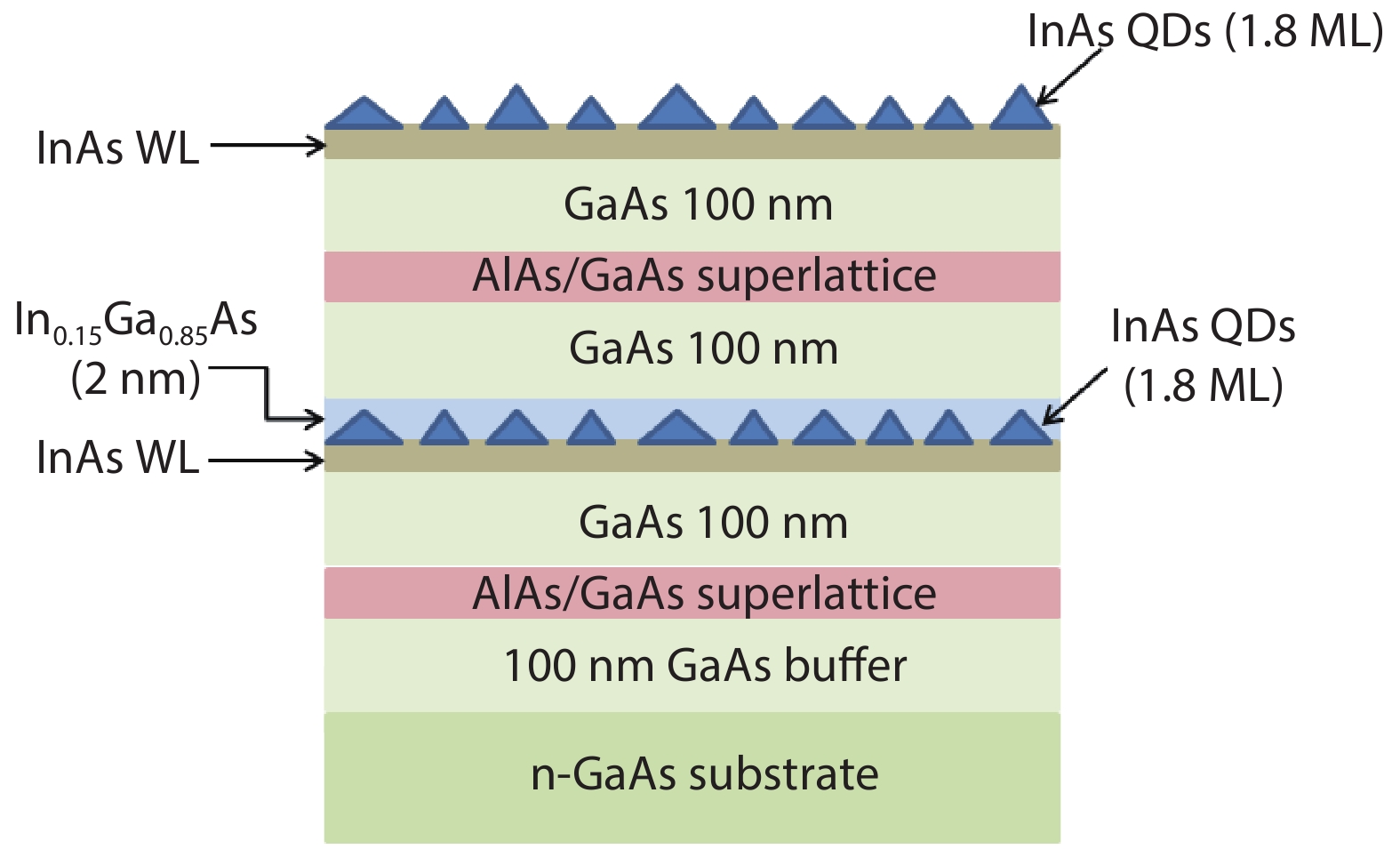
The InAs/GaAs QDs sample was grown on the semi-insulated GaAs (001) substrate by a Riber 32P solid source MBE system. Firstly, a 100 nm GaAs buffer layer and bottom barrier layer were successively grown on the GaAs substrate at 580 °C. Next, the temperature of the substrate was quickly cooled down to 500 °C to deposit 1.8 monolayer (ML) InAs QDs, which were covered by In0.15Ga0.85As SRL with a thickness of 2 nm. Then, a 100 nm GaAs upper barrier layer was grown at 580 °C. 10-cycle 2 nm AlAs/2 nm GaAs superlattices (SLS) were grown before and after the deposition of the GaAs barrier layer to prevent photo-generated charge carriers from diffusing to the substrate to reach the surface. Finally, a 100 nm GaAs layer and an uncapped QDs layer identical to the buried layer were grown on the AlAs/GaAs SLS. Fig. 1 shows the schematic of InAs/GaAs QDs sample heteroepitaxy structure.
![]()
Figure 1.(Color online) Schematic for the heteroepitaxy structure of InAs/GaAs QDs.
Our samples, cut from the central region of the as-grown epitaxial layer were subjected to RTA treatment in AccuThermo AW 610 system for 60 s in a nitrogen atmosphere at the annealing temperature TRTA = 750, 800, 850 and 900 °C, respectively. During the RTA process, a GaAs wafer was used to cover these samples in order to prevent the samples from degradation due to arsenic volatilization from the surface at high temperature.
Samples were mounted in an enclosed circulating Helium cryostat, which allowed for tuning the temperature from 16 to 300 K. Temperature-dependent PL measurements were performed on all the samples using a 633 nm excitation wavelength under 14 mW of power. Then, the power-dependent PL measurement was performed, with an Nd:YAG laser of 532 nm at 300 K, on the annealed samples, as well as the as-grown sample.
3. Results and discussion
Fig. 2(a) demonstrates the PL spectrum of InAs/GaAs QDs in the as-grown sample recorded at the temperatures of 16 and 300 K, respectively, under 14 mW of excitation power. As shown in the figure, the full width at half maximum (FWHM) of these two PL spectra were 133.35 meV (16 K) and 196.18 meV (300 K), respectively. As usual, the PL intensity significantly decreased with the increase of temperature from 16 to 300 K, accompanied with the peak energy shifting from 1.155 eV at 16 K to 1.068 eV at 300 K. Besides, the PL spectrum of the as-grown InAs QDs at both 16 and 300 K was apparently asymmetric, with an obvious shoulder at the high-energy side of the PL peak.
![]()
Figure 2.(Color online) (a) The PL spectrum of the as-grown QDs sample under 14 mW of excitation power at 16 and 300 K respectively. (b) The Gaussian fitting diagram of the PL spectrum of the as-grown QDs sample at 16 K, with the dash-dot lines showing the Gaussian fitting of different emission peaks.
Fig. 2(b) shows a Gaussian fitting diagram of QDs PL spectrum at 16 K. As illustrated by the dash-dot lines in Fig. 2(b), the asymmetric PL spectrum of QDs at 16 K can be well fitted using two Gaussian type functions with peaks at 1.153 and 1.197 eV respectively. In particular, the spacing between both Gaussian peaks was estimated to be around 44 meV, which was significantly smaller than the typical value (60–80 meV) of the energy separation between the GS and first excited state of an InAs QD in a population of InAs QDs[
Figs. 3(a) and 3(b) present the normalized PL spectrum of as-grown and RTA-treated QDs samples with TRTA = 750, 800, 850 and 900 °C respectively at the temperatures of 16 and 300 K. As shown in both figures, all annealed QDs samples exhibited a distinct blue-shift in the PL spectrum (measured at the temperatures of 16 and 300 K) compared with as-grown QDs. Fig. 3(a) shows that in the PL spectrum at T = 16 K the main peak position of the QDs annealed at 750 °C was observed to be at 1.269 eV, which was blue shifted by 113 meV compared with that of the as-grown QDs (1.156 eV). However, the PL peak in the QDs annealed at T = 800 and 850 °C were blue shifted by 108.37 and 97.23 meV, respectively, which was slightly less than the RTA-induced blue-shift in the PL spectrum of the QDs annealed at 750 °C. Meanwhile, it can be observed that the sample annealed at 900 °C presented the largest blue-shift (169 meV). This behavior was completely different from other reports in the literature, to our knowledge, that the RTA-induced blue-shift increased significantly with the increase of annealing temperature[
![]()
Figure 3.(Color online) The normalized PL spectra of as-grown QDs and QDs annealed at various temperatures obtained at (a) 16 K and (b) 300 K under an excitation power of 14 mW. Inset: The PL peak energy of QDs at (a)
Furthermore, the PL peak energy of different-sized QDs was shown as a function of the RTA temperature in the insets of Figs. 3(a) and 3(b), and the similar variation trends were observed with the increase of annealing temperature.
In addition, the peak shape of the PL spectrum of the QDs sample subjected to RTA presented a slight modification. At 16 K, the asymmetry of the PL spectrum peak shape of samples annealed below 850 °C decreased with the increase of annealing temperature. The peak shape of the PL spectrum became sharper with annealing temperature increased to 900 °C. What is more, it was found that the PL spectrum of QDs annealed at 850 °C produced a new spectral peak at 1.354 eV compared with that of as-grown QDs. Moreover, it can be seen that the PL spectrum was significantly broadened when the temperature of PL measurements rose to 300 K. Therefore, the PL spectra in Fig. 3 were fitted by Gaussian fitting, and the curves of PL spectral width and integrated PL intensity versus annealing temperature were plotted as shown in Fig. 4.
![]()
Figure 4.(Color online) (a) The PL spectral width of QDs at
Fig. 4(a) showed the PL spectral width of the RTA-treated QDs with the change of annealing temperature, measured at both T = 16 and 300 K. At 16 K, the PL spectral width of the QDs sample annealed at up to 750 °C was greater than that of the as-grown sample, which implied that RTA did not always induce the narrowing of PL spectral peaks. The PL spectral width of the samples annealed at 800 °C saw a sharp decline, which indicated that RTA treated InAs/GaAs QDs at an annealing temperature of 800 °C had relatively excellent crystal quality. With the further increase of annealing temperature, the PL spectral width increased, then decreased and obtained the minimum value at 900 °C. At 300 K, it can be observed that the PL spectral width changed from 216.4 meV to 240.86 meV with the increase of annealing temperature from 750 to 800 °C. Compared with as-grown QDs, QDs saw an increase of 44.68 meV in PL spectral width after being annealed at 800 °C. This result indicated that the electron–phonon scattering effect and thermal distribution had a significant impact on annealed samples with different QDs densities, leading to the significant broadening of PL spectrum[
Fig. 4(b) shows the integrated PL intensity of PL peak emission with the change of annealing temperature. The integrated PL intensity of RTA-treated samples at an annealing temperature of 750 °C and above saw a slight drop at 300 K, which was caused by the weakening of carrier confinement ability and the thermal excitation of more photo-generated carriers in QDs into the InAs WL or GaAs barrier layer. At low temperature (16 K), however, the integrated PL intensity was enhanced as samples were annealed at 850 °C, which might result from the reduction of non-radiative recombination and the contribution of lower thermal energy to increasing the integrated PL intensity of annealed QDs. The integrated PL intensity of QDs annealed at 900 °C was greatly attenuated owing to the partial dissolution of QDs and the degradation of the crystal quality of samples at high temperatures.
As mentioned above, the PL spectrum of the QDs subjected to RTA treatment showed a significant inhomogeneous broadening at 300 K, especially for the sample RTA-treated at 800 °C. And that, there are new peaks on the PL high energy side of all samples as shown in Figs. 3(b). To identify the source of the PL spectrum and explain its broadening, a power-dependent PL experiment was performed on all annealed samples. The upper half of Figs. 5(a)–5(d) demonstrates the PL spectrum of four annealed samples at 300 K as a function of excitation power from 4 to 135 mW. For data analysis, the PL spectrum of all annealed samples under the excitation power of 40 mW was extracted and Gaussian fitting was performed for data analysis. As shown in the lower half of Figs. 5(a)–5(d), the PL spectrum of four annealed samples was composed of four spectral peaks, namely P1, P2, P3 and P4.
![]()
Figure 5.(Color online) The top half of the figure shows the power-dependent PL spectrum of samples annealed at (a) 750, (b) 800, (c) 850, and (d) 900 °C recorded at 300 K. The PL spectrum of the annealed sample under an excitation power of 40 mW was extracted and Gaussian fitting was performed, as shown in the lower part of the figure.
Figs. 5(a) and 5(b) show that the peak intensities of the four spectral peaks P1, P2, P3 and P4 of RTA treated samples at an annealing temperature of 750 and 800 °C almost all decreased at a constant ratio. All spectral peaks existed even under the lowest excitation power, suggesting that these peaks were not derived from the luminescence of the excited state of QDs. In the PL spectrum, the first two peaks (P1 and P2) in the low-energy region showed the size distribution of QDs corresponding to the GS luminescence of QDs with different sizes. The increase of test temperature to 300 K resulted in the thermal excitation of some carriers in QDs into the WL where radiative or non-radiative recombination occurred. Therefore, the third peak (P3) in the high-energy region was the luminescence peak of the QDs WL, which had a relatively small FWHM. Besides, it was suggested the fourth peak (P4) at the high-energy side of the spectrum might be generated from the In0.15Ga0.85As SRL. Thus, it can be seen that the broadening of the PL spectrum of QDs annealed at 750 and 800 °C was associated with the GS emission of different-sized QDs and the emission of the WL and SRL.
Figs. 5(c) and 5(d) are the PL spectrum and Gaussian fitting diagrams of InAs/GaAs QDs annealed at 850 and 900 °C, respectively. Based on Gaussian fitting, four peaks can be clearly defined on the high-energy side of PL spectrum, while the low energy side (1.165 eV) of the PL spectrum is related to the laser. For this kind of QD sample annealed at a higher temperature (850 or 900 °C), the lateral sizes of the QDs increased with increasing RTA temperature and the partial QDs dissolved into the surrounding WL, resulting in a modified WL and a gradual conversion of InAs QDs to an InGaAs QW structure[
4. Conclusions
In summary, PL measurements were performed to investigate the effect of RTA treatment on the optical performance of self-assembled InAs/GaAs QDs. It was found that the variation in the PL blue-shift of InAs/GaAs QDs as a function of annealing temperature was associated with the reduction of strain between QDs and GaAs barrier layers after RTA and the inter-diffusion of In and Ga atoms at specific annealing temperatures. In addition, the PL spectrum could be broadened effectively by RTA at 300 K. The PL spectral width of the QDs sample annealed at 800 °C was 240.86 meV, which was obviously higher than that of the as-grown sample (196.18 meV). This feature of annealed samples is very applicable to optical coherence tomography. Therefore, this study broadened the PL spectrum of InAs/GaAs QDs by RTA.
Acknowledgements
This work was supported by the National Key Research and Development Program of China (Grant No. 2016YFB0402404), the National Natural Science Foundation of China (Grant No. 21972103), Key Research and Development Program of Shanxi Province (Grant No. 201703D111026), and the Beijing Municipal Science and Technology Commission (Grant No. Z181100004418009).
References
[1] P Bhattacharya, K Kamath, J Singh et al. In(Ga)As/GaAs self-organized quantum dot lasers: DC and small-signal modulation properties. IEEE Trans Electron Devices, 46, 871(2017).
[2] D. Bimberg. Quantum dots for lasers, amplifiers and computing. J Phys D, 38, 2055(2005).
[3] K A Sablon, J W Little, V Mitin et al. Strong enhancement of solar cell efficiency due to quantum dots with built-in charge. Nano Lett, 11, 2311(2011).
[4] V P Deviprasad, H Ghadi, D Das et al. High performance short wave infrared photodetector using p –i –p quantum dots (InAs/GaAs) validated with theoretically simulated model. J Alloys Compd, 804, 18(2019).
[5] O Karni, K J Kuchar, A Capua et al. Carrier dynamics in inhomogeneously broadened InAs/AlGaInAs/InP quantum-dot semiconductor optical amplifiers. Appl Phys Lett, 104, 121104(2014).
[6] Y Ebiko, S Muto, D Suzuki et al. Island size scaling in InAs/GaAs self-assembled quantum dots. Phys Rev Lett, 80, 2650(1998).
[7] Z Y Zhang, R A Hogg, X Q Lv et al. Self-assembled quantum-dot superluminescent light-emitting diodes. Adv Opt Photonics, 2, 201(2010).
[8] Z Z Sun, D Ding, Q Gong et al. Quantum-dot superluminescent diode: A proposal for an ultra-wide output spectrum. Opt Quantum Electron, 31, 1235(1999).
[9] N Ozaki, K Takeuchi, S Ohkouchi et al. Monolithically grown multi-color InAs quantum dots as a spectral-shape-controllable near-infrared broadband light source. Appl Phys Lett, 103, 051121(2013).
[10] W Li, S Chen, J Wu et al. The effect of post-growth rapid thermal annealing on InAs/InGaAs dot-in-a-well structure monolithically grown on Si. J Appl Phys, 125, 135301(2019).
[11] S Sengupta, N Halder, S. Chakrabarti. Effect of post-growth rapid thermal annealing on bilayer InAs/GaAs quantum dot heterostructure grown with very thin spacer thickness. Mater Res Bull, 45, 1593(2010).
[12] M Triki, S Jaziri, R. Bennaceur. Optical transitions of InAs/GaAs quantum dot under annealing process. J Appl Phys, 111, 104304(2012).
[13] S Saravanan, T. Harayama. Improvement in size distribution and optical properties of InAs/GaAs QDs by post growth thermal treatment. Phys Status Solidi B, 246, 725(2009).
[14] S Adhikary, S. Chakrabarti. A detailed investigation on the impact of post-growth annealing on the materials and device characteristics of 35-layer In0.50Ga0.50As/GaAs quantum dot infrared photodetector with quaternary In0.21Al0.21Ga0.58As capping. Mater Res Bull, 47, 3317(2012).
[15] S Adhikary, S. Chakrabarti. Spectral broadening due to post-growth annealing of a long-wave InGaAs/GaAs quantum dot infrared photodetector with a quaternary barrier layer. Thin Solid Films, 552, 146(2014).
[16] H S Djie, D N Wang, B S Ooi et al. Emission wavelength trimming of self-assembled InGaAs/GaAs quantum dots with GaAs/AlGaAs superlattices by rapid thermal annealing. Thin Solid Films, 515, 4344(2007).
[17] M Rossetti, L Li, A Markus et al. Characterization and modeling of broad spectrum InAs–GaAs quantum-dot superluminescent diodes emitting at 1.2–1.3
[18] U H Lee, Y D Jang, H Lee et al. The energy level spacing between the ground and first excited states in InAs/GaAs quantum dots as a measure of the zero dimensionality. Physica E, 17, 129(2003).
[19] K Ghosh, S Kundu, N Halder et al. Annealing of In0.45Ga0.55As/ GaAs quantum dots overgrown with large monolayer (11 ML) coverage for applications in thermally stable optoelectronic devices. Solid State Commun, 151, 1394(2011).
[20] J S Kim, J H Lee, S U Hong et al. Structural and optical properties of shape-engineered InAs quantum dots. J Appl Phys, 94, 2486(2003).
[21] A Agarwal, M Srujan, S Chakrabarti et al. Investigation of thermal interdiffusion in InAs/In0.15Ga0.85As/GaAs quantum dot-in-a-well heterostructures. J Lumin, 143, 96(2013).
[22] S Shah, K Ghosh, S Jejurikar et al. Ground-state energy trends in single and multilayered coupled InAs/GaAs quantum dots capped with InGaAs layers: Effects of InGaAs layer thickness and annealing temperature. Mater Res Bull, 48, 2933(2013).
[23] W Lei, Y H Chen, Y L Wang et al. Influence of rapid thermal annealing on InAs/InAlAs/InP quantum wires with different InAs deposited thickness. J Cryst Growth, 284, 20(2005).
[24] A Babiński, J Jasiński, R Bożek et al. Rapid thermal annealing of InAs/GaAs quantum dots under a GaAs proximity cap. Appl Phys Lett, 79, 2576(2001).

Set citation alerts for the article
Please enter your email address
© Copyright 2018-2021 | Chinese Laser Press. All Rights Reserved 沪ICP备15018463号-20