• Acta Physica Sinica
  • Vol. 68, Issue 22, 228501-1 (2019)
Jian-Bin Kang1、2、*, Qian Li1、2, and Mo Li1、2
Author Affiliations
  • 1Microsystem and Terahertz Research Center, China Academy of Engineering Physics, Chengdu 610200, China
  • 2Insititute of Electronic Engineering, China Academy of Engineering Physics, Mianyang 621999, China
  • show less
    DOI: 10.7498/aps.68.20190722 Cite this Article
    Jian-Bin Kang, Qian Li, Mo Li. Effects of material structure on device efficiency of III-nitride intersubband photodetectors[J]. Acta Physica Sinica, 2019, 68(22): 228501-1 Copy Citation Text show less
    Conduction band profile and electron distribution for typical photovoltaic nitride intersubband photodetectors, with ten periods, twenty periods and fifty periods of GaN/AlN quantum wells, respectively. The inset shows the schematic image of the sample structure.典型光伏型GaN/AlN子带跃迁探测器量子阱周期数分别为10, 20, 50情况下的导带结构和电子浓度分布, 左下侧的插图为器件材料结构示意图
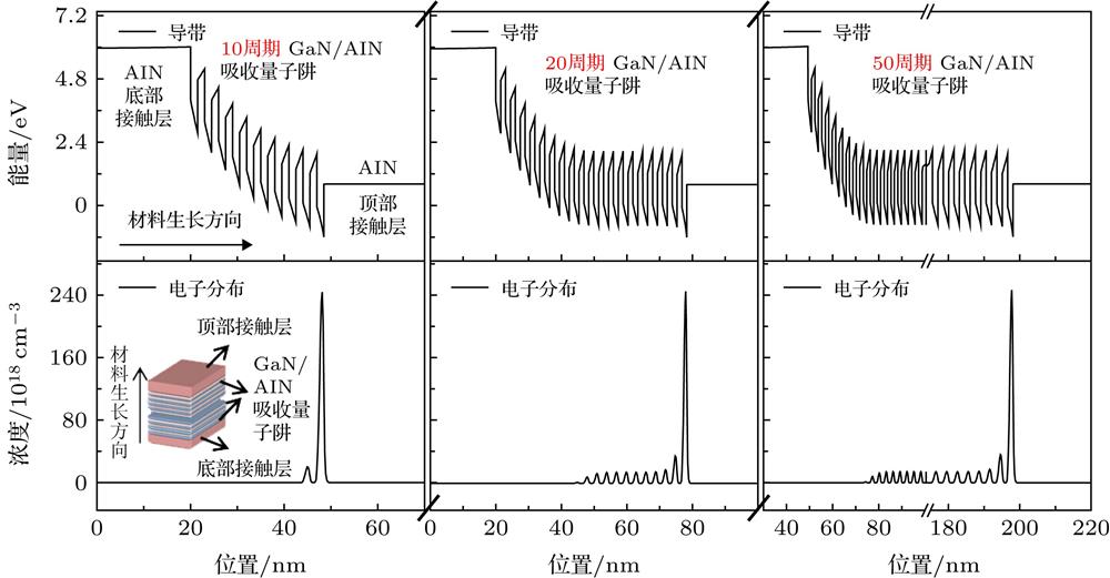
    Fig. 1. Conduction band profile and electron distribution for typical photovoltaic nitride intersubband photodetectors, with ten periods, twenty periods and fifty periods of GaN/AlN quantum wells, respectively. The inset shows the schematic image of the sample structure.典型光伏型GaN/AlN子带跃迁探测器量子阱周期数分别为10, 20, 50情况下的导带结构和电子浓度分布, 左下侧的插图为器件材料结构示意图
    Conduction band profile and electron distribution for typical photovoltaic nitride intersubband photodetectors doped to 5 × 1018 cm–3, 2 × 1019 cm–3 and 5 × 1019 cm–3 in quantum wells, respectively.典型光伏型GaN/AlN子带跃迁探测器量子势阱掺杂浓度分别为5 × 1018 cm–3, 2 × 1019 cm–3和5 × 1019 cm–3情况下的导带结构和电子浓度分布
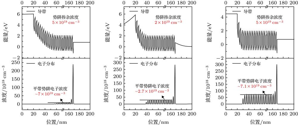
    Fig. 2. Conduction band profile and electron distribution for typical photovoltaic nitride intersubband photodetectors doped to 5 × 1018 cm–3, 2 × 1019 cm–3 and 5 × 1019 cm–3 in quantum wells, respectively. 典型光伏型GaN/AlN子带跃迁探测器量子势阱掺杂浓度分别为5 × 1018 cm–3, 2 × 1019 cm–3和5 × 1019 cm–3情况下的导带结构和电子浓度分布
    Conduction band profile and electron distribution for typical photovoltaic nitride intersubband photodetectors, with GaN, Al0.5Ga0.5N and AlN contact layers, respectively.典型光伏型GaN/AlN子带跃迁探测器分别采用GaN, Al0.5Ga0.5N和AlN材料作为接触层情况下的导带结构和电子浓度分布
    Fig. 3. Conduction band profile and electron distribution for typical photovoltaic nitride intersubband photodetectors, with GaN, Al0.5Ga0.5N and AlN contact layers, respectively. 典型光伏型GaN/AlN子带跃迁探测器分别采用GaN, Al0.5Ga0.5N和AlN材料作为接触层情况下的导带结构和电子浓度分布
    Conduction band profile and squared envelope functions for terahertz intersubband photodetectors based on (a) a single barrier and a single well structure and (b) a double-step structure.基于(a)单一量子阱结构和(b)双台阶量子阱结构的太赫兹波段氮化物子带跃迁探测器能带结构和电子波函数分布
    Fig. 4. Conduction band profile and squared envelope functions for terahertz intersubband photodetectors based on (a) a single barrier and a single well structure and (b) a double-step structure.基于(a)单一量子阱结构和(b)双台阶量子阱结构的太赫兹波段氮化物子带跃迁探测器能带结构和电子波函数分布
    (a) Barrier layer polarization fields and (b) well layer polarization fields as a function of Al mole composition of barrier layer (xbr) for double-step devices.双台阶结构器件中势垒层电场(a)和势阱层电场(b)随势垒层Al组分变化的关系
    Fig. 5. (a) Barrier layer polarization fields and (b) well layer polarization fields as a function of Al mole composition of barrier layer (xbr) for double-step devices. 双台阶结构器件中势垒层电场(a)和势阱层电场(b)随势垒层Al组分变化的关系
    The influence of each layer thickness on the barrier layer polarization fields (right ordinates) and the change of Al mole composition of barrier under the condition that the polarization field in barrier layer is kept at zero (left ordinates) for double-step devices.双台阶结构器件中势垒层极化电场随各层材料厚度变化的关系(右侧纵坐标), 以及为了保持势垒层中极化电场始终为零, 势垒层Al组分随厚度的变化关系(左侧纵坐标)
    Fig. 6. The influence of each layer thickness on the barrier layer polarization fields (right ordinates) and the change of Al mole composition of barrier under the condition that the polarization field in barrier layer is kept at zero (left ordinates) for double-step devices.双台阶结构器件中势垒层极化电场随各层材料厚度变化的关系(右侧纵坐标), 以及为了保持势垒层中极化电场始终为零, 势垒层Al组分随厚度的变化关系(左侧纵坐标)
    Transmission coefficient as a function of energy for double-step devices: (a) With different Al mole compositions of step barrier layer; (b) with different thicknesses of step barrier layer.双台阶结构器件台阶势垒层Al组分(a)和厚度(b)不同时载流子隧穿透过率随载流子能量的变化关系
    Fig. 7. Transmission coefficient as a function of energy for double-step devices: (a) With different Al mole compositions of step barrier layer; (b) with different thicknesses of step barrier layer.双台阶结构器件台阶势垒层Al组分(a)和厚度(b)不同时载流子隧穿透过率随载流子能量的变化关系
    Jian-Bin Kang, Qian Li, Mo Li. Effects of material structure on device efficiency of III-nitride intersubband photodetectors[J]. Acta Physica Sinica, 2019, 68(22): 228501-1
    Download Citation