• Acta Physica Sinica
  • Vol. 68, Issue 22, 228501-1 (2019)
Jian-Bin Kang1、2、*, Qian Li1、2, and Mo Li1、2
Author Affiliations
  • 1Microsystem and Terahertz Research Center, China Academy of Engineering Physics, Chengdu 610200, China
  • 2Insititute of Electronic Engineering, China Academy of Engineering Physics, Mianyang 621999, China
  • show less
    DOI: 10.7498/aps.68.20190722 Cite this Article
    Jian-Bin Kang, Qian Li, Mo Li. Effects of material structure on device efficiency of III-nitride intersubband photodetectors[J]. Acta Physica Sinica, 2019, 68(22): 228501-1 Copy Citation Text show less

    Abstract

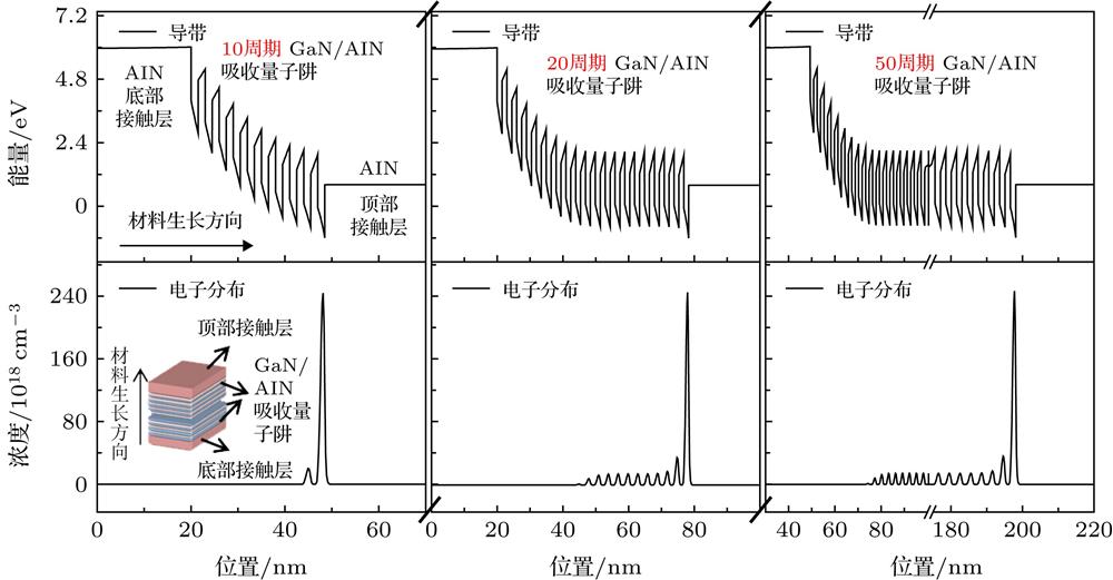
    The photodetection potential applications of III-nitride semiconductor are not only restricted in the ultraviolet range, but also extended to the infrared and even terahertz wave range through intersubband transition (ISBT) process between quantum-confined electronic states. The large conduction band offset (~1.75 eV for GaN/AlN heterostructures) and the strong electron-phonon interaction in these materials enable the III-nitride ISBT photodetectors to operate with ultrahigh speed for near-infrared telecommunication applications. Furthermore, due to the large energy of longitudinal optical phonons of nitride materials (~92 meV for GaN), the corresponding ISBT photodetectors are demonstrated as a promising candidate for operating in a specific terahertz (THz) range (5-12 THz) at high temperature, which is fundamentally in accessible to As-based devices. One of the major difficulties in realizing high performance III-nitride ISBT photodetectors is the existence of undesired polarization field inherited from conventional c-axis nitrides, which greatly makes the design complicated. In this paper, we theoretically study the influences of critical material structure parameters on the band structure, electron distribution, polarization field intensity, and tunneling effect based on near-infrared photovoltaic photodetectors and terahertz double-step photodetectors.III-nitride ISBT photodetectors operating in near-infrared are designed to be able to suppress the internal electric field in the active region, so that as many quantum wells as possible can be populated by electrons to enhance the absorption efficiency. It is found that with the increase of well periods and well doping concentration, a weaker average polarization field is observed, and as a result more wells will be populated with electrons. In addition, keeping the lattice constant of the contact layer material the same as the average lattice constant of the active region is beneficial to making more quantum wells effectively populated with electrons. On the other hand, the devices operating in a terahertz range require a more accurate design of energy band than the near-infrared ones due to its rather small energy interval. The design difficulties lie in how to ensure both the efficient absorption of photons and the following transportation of photo-excited electrons in the presence of polarization-induced field. The simulation results indicate that the polarization field in an active region is sensitive to the aluminum mole composition of barrier layer, the thickness of step well and step barrier layers, while even if the thickness of well and barrier layers change, the polarization field in barrier layer will stay the same. Moreover, reducing the aluminum mole composition of step barrier layer or appropriately increasing its thickness will be helpful in enhancing the photo-excited electrons tunneling. The above knowledge is beneficial to the optimal design of III-nitride ISBT photodetectors with high efficiency.
    Jian-Bin Kang, Qian Li, Mo Li. Effects of material structure on device efficiency of III-nitride intersubband photodetectors[J]. Acta Physica Sinica, 2019, 68(22): 228501-1
    Download Citation