• Opto-Electronic Advances
  • Vol. 5, Issue 4, 210015 (2022)
Xiao He1、†, Donglin Liu1、†, Hongfei Wang2, Liheng Zheng1, Bo Xu3, Biye Xie2、4, Meiling Jiang1, Zhixin Liu1, Jin Zhang3, Minghui Lu2, and Zheyu Fang1、*
Author Affiliations
  • 1School of Physics, State Key Lab for Mesoscopic Physics, Academy for Advanced Interdisciplinary Studies, Collaborative Innovation Center of Quantum Matter, and Nano-optoelectronics Frontier Center of Ministry of Education, Peking University Yangtze Delta Institute of Optoelectronics, Peking University, Beijing 100871, China
  • 2National Laboratory of Solid State Microstructures, Department of Materials Science and Engineering, Nanjing University, Nanjing 210093, China
  • 3College of Chemistry and Molecular Engineering, Peking University, Beijing 100871, China
  • 4Department of Physics and HKU-UCAS Joint Institute for Theoretical and Computational Physics at Hong Kong, the University of Hong Kong, Pokfulam Road, Hong Kong, China
  • show less
    DOI: 10.29026/oea.2022.210015 Cite this Article
    Xiao He, Donglin Liu, Hongfei Wang, Liheng Zheng, Bo Xu, Biye Xie, Meiling Jiang, Zhixin Liu, Jin Zhang, Minghui Lu, Zheyu Fang. Field distribution of the Z2 topological edge state revealed by cathodoluminescence nanoscopy[J]. Opto-Electronic Advances, 2022, 5(4): 210015 Copy Citation Text show less
    The design and band structure of the proposed Z2 PTI. (a–c) Schematic of undeformed, shrunken, and expanded PhCs with their calculated band structures. The dashed hexagon outlines the structure unit cell, and the white triangle represents the hole area. The lattice constant a = 444 nm, the length of triangular hole l = 154 nm. The distance r between the unit cell center and triangular hole centroid for shrunken PhC is 138 nm, and for expanded PhC is 160 nm. The graphene-like band structure is formed when r = a/3 (undeformed), and topological trivial and non-trivial bandgaps can be opened at Γ point, when r < a/3 (shrunken) and r > a/3 (expanded), respectively. (d) Pseudo-colored SEM image of a fabricated structure. The outside shrunken and inside expanded PhCs are identified by blue and red regions, respectively. (e) Zoom-in SEM image of the interface area. Black dashed lines identify the unit cell of shrunken and expanded PhCs.
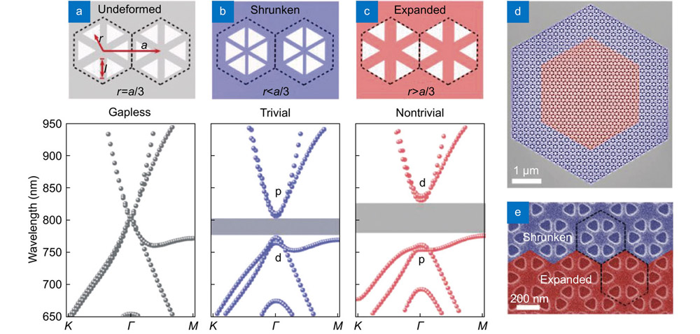
    Fig. 1. The design and band structure of the proposed Z2 PTI. (ac) Schematic of undeformed, shrunken, and expanded PhCs with their calculated band structures. The dashed hexagon outlines the structure unit cell, and the white triangle represents the hole area. The lattice constant a = 444 nm, the length of triangular hole l = 154 nm. The distance r between the unit cell center and triangular hole centroid for shrunken PhC is 138 nm, and for expanded PhC is 160 nm. The graphene-like band structure is formed when r = a/3 (undeformed), and topological trivial and non-trivial bandgaps can be opened at Γ point, when r < a/3 (shrunken) and r > a/3 (expanded), respectively. (d) Pseudo-colored SEM image of a fabricated structure. The outside shrunken and inside expanded PhCs are identified by blue and red regions, respectively. (e) Zoom-in SEM image of the interface area. Black dashed lines identify the unit cell of shrunken and expanded PhCs.
    Characterization of the Z2 topological edge state and its dark line. (a) Optical image of the fabricated Z2 PTI with a WSe2 monolayer transferred on the top. The interface between shrunken and expanded PhC regions, and the area of WSe2 monolayer fringe are marked with white and gray dashed lines, respectively. (b) PL spectra collected from the WSe2 monolayer upon the shrunken PhC (blue), expanded PhC (red), and near interface (green). The yellow shadow indicates the overlapped bandgap of shrunken and expanded PhCs. (c–e) PL mappings of bulk (expanded)-edge-bulk (shrunken) state at the resonance wavelength of 778 nm, 788 nm, and 802 nm. The defect triangle region of the WSe2 monolayer arises from the transferring process, like a wrinkle of the WSe2 monolayer, resulting in a bright triangle region in Fig. 2(c–e).
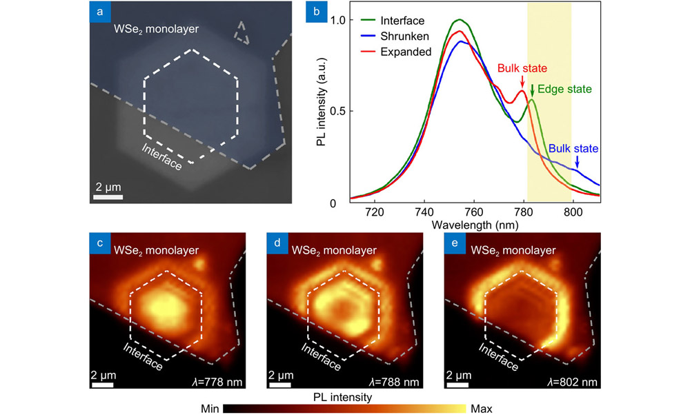
    Fig. 2. Characterization of the Z2 topological edge state and its dark line. (a) Optical image of the fabricated Z2 PTI with a WSe2 monolayer transferred on the top. The interface between shrunken and expanded PhC regions, and the area of WSe2 monolayer fringe are marked with white and gray dashed lines, respectively. (b) PL spectra collected from the WSe2 monolayer upon the shrunken PhC (blue), expanded PhC (red), and near interface (green). The yellow shadow indicates the overlapped bandgap of shrunken and expanded PhCs. (ce) PL mappings of bulk (expanded)-edge-bulk (shrunken) state at the resonance wavelength of 778 nm, 788 nm, and 802 nm. The defect triangle region of the WSe2 monolayer arises from the transferring process, like a wrinkle of the WSe2 monolayer, resulting in a bright triangle region in Fig. 2(c–e).
    Deep-subwavelength LDOS imaging of the dark line of edge state. (a-d) CL mapping of four samples with increasing l to show the change of structure radiative LDOS. (e) Corner SEM image of the same sample in (b), the interface of two PhCs is marked with a solid green line. (f) Corresponding CL mapping of (e). The right part of the interface of two PhCs is marked with a solid white line. The inset is a detailed CL image of a single unit cell.
    Fig. 3. Deep-subwavelength LDOS imaging of the dark line of edge state. (a-d) CL mapping of four samples with increasing l to show the change of structure radiative LDOS. (e) Corner SEM image of the same sample in (b), the interface of two PhCs is marked with a solid green line. (f) Corresponding CL mapping of (e). The right part of the interface of two PhCs is marked with a solid white line. The inset is a detailed CL image of a single unit cell.
    Simulation of edge states. (a) Schematic of the interface that consists of expanded and shrunken PhCs. The interface of shrunken and expanded PhCs is marked as a zig-zag line. (b) Calculated band structure of the interface area. (c–d) Simulated expanded bulk state magnetic field (Hz) and electric intensity (|E|2) distributions at 778 nm (z = 0). (e–h) Simulated Z2 topological edge state magnetic field (Hz) and electric intensity (|E|2) distributions at 788 nm and 804 nm (z = 0). The upper (bottom) right-side of (e) and (g) shows an enlarged magnetic field of the unit cell 2 (3) and a general quadrupolar (dipolar) mode respectively. Parameters used in Fig. 4 are the same as parameters used in Fig. 1.
    Fig. 4. Simulation of edge states. (a) Schematic of the interface that consists of expanded and shrunken PhCs. The interface of shrunken and expanded PhCs is marked as a zig-zag line. (b) Calculated band structure of the interface area. (cd) Simulated expanded bulk state magnetic field (Hz) and electric intensity (|E|2) distributions at 778 nm (z = 0). (eh) Simulated Z2 topological edge state magnetic field (Hz) and electric intensity (|E|2) distributions at 788 nm and 804 nm (z = 0). The upper (bottom) right-side of (e) and (g) shows an enlarged magnetic field of the unit cell 2 (3) and a general quadrupolar (dipolar) mode respectively. Parameters used in Fig. 4 are the same as parameters used in Fig. 1.
    Xiao He, Donglin Liu, Hongfei Wang, Liheng Zheng, Bo Xu, Biye Xie, Meiling Jiang, Zhixin Liu, Jin Zhang, Minghui Lu, Zheyu Fang. Field distribution of the Z2 topological edge state revealed by cathodoluminescence nanoscopy[J]. Opto-Electronic Advances, 2022, 5(4): 210015
    Download Citation