Abstract
![]()
Photonic topological insulators with robust boundary states can enable great applications for optical communication and quantum emission, such as unidirectional waveguide and single-mode laser. However, because of the diffraction limit of light, the physical insight of topological resonance remains unexplored in detail, like the dark line that exists with the crystalline symmetry-protected topological edge state. Here, we experimentally observe the dark line of the Z2 photonic topological insulator in the visible range by photoluminescence and specify its location by cathodoluminescence characterization, and elucidate its mechanism with the p-d orbital electromagnetic field distribution which calculated by numerical simulation. Our investigation provides a deeper understanding of Z2 topological edge states and may have great significance to the design of future on-chip topological devices.
Introduction
Topology as a mathematic concept that is concerned with invariant properties under continuous deformation was introduced into physics to describe the global property of a physical system, motivating enormous research interests in modern electronics1, 2, phononics3, 4, and nanophotonics5-7. Substantial efforts have been devoted towards realizing photonic topological insulators (PTIs), such as the photonic superlattice8, gyromagnetic rod array9, 10, metacrystal11, and coupled resonators12, 13, which characterized by unprecedented topological edge states that were observed at the interface between two topologically distinct materials. Topological edge states have shown great potentials to the unidirectional propagation without backscattering14, 15, and used to enhance the nonlinear light generation16. For the single-mode laser application, the topological edge state is robust and insensitive to the fabrication defect, and has been successfully used to saturate the gain to prevent other resonant modes from lasing17-20.
Besides the classical electromagnetic realm, PTIs also can be utilized in the quantum domain21, by coupling with light at the single-photon level. A Z2 PTI, which possesses two robust pseudo-spin states, was theoretically proposed based on the crystalline symmetry22, and then followed by a specific TE mode design based on an all-dielectric slab23. Such design is considered naturally compatible with the semiconductor technology, and shows on-chip integration capability for the unidirectional topological waveguide24, 25 and single-mode spin-momentum-locked laser26. However, a defective dark line was found to exist with the Z2 topological edge state24-27, which may affect the propagation distance of waveguide mode and the threshold intensity of single-mode lasing. Therefore, an understanding about the dark line of Z2 topological edge states is urgent for future topological device designs and applications.
Due to the optical diffraction limit, it is difficult to investigate the topological edge state by using traditional optical microscopy. As a non-invasive detection method, cathodoluminescence (CL) microscopy with nanoscale spatial resolution and precise electron impinging position has been successfully applied for the electromagnetic field study, such as the dispersion and optical local density of state (LDOS) of the photonic crystal (PhC)28-30 and metallic nanostructures31, 32. The LDOS is an intrinsic characteristic of PhC, and can be used to provide a deep-subwavelength detail of the topological edge state. To our knowledge, the LDOS of topological edge state has not been reported yet.
In this work, we realize the Z2 topological edge state in the visible range and characterize its dark line with the CL nanoscopy, and then elucidate it with the PhC p-d orbital field distribution that is simulated by varFDTD solutions. The Z2 topological edge state can be directly imaged from the designed PhC structure with the enhanced photoluminescence (PL) of the WSe2 monolayer that covered on the top. To precisely image the dark line, the radiative LDOS of the edge state is further characterized by using CL nanoscopy. And the dark line can be interpreted with the artificial p-d orbital field distribution by analyzing simulated Z2 topological edge states in detail. Our study provides a deeper understanding of Z2 topological edge states, and may have great significance for future topological applications, especially quantum emission.
Results and discussion
The design and characterization of Z2 PTI.
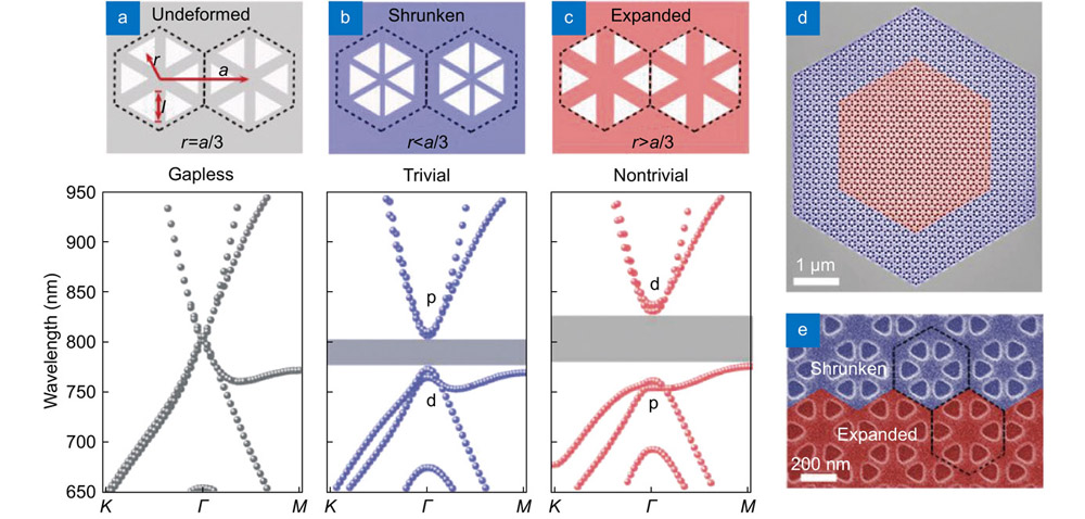
With the symmetry-protected approach proposed by Wu22 and Barik 23, our Z2 PTI that consists of PhC structures with triangular holes arranged in a honeycomb lattice possesses two Dirac cones at K and K’ points in the momentum space. Considering a unit cell as a triangular lattice with six holes, the Dirac cone of the honeycomb lattice is folded to doubly degenerate at Γpoint, as shown in the band structure of Fig. 1(a). By keeping the whole structure as C6v symmetry, shrunken and expanded PhCs can be designed by slightly decreasing or increasing the distance between unit cell center and triangular hole centroid. Intracell and intercell interactions are strengthened in the shrunken and expanded PhCs respectively, which result in corresponding topological trivial and non-trivial bandgaps at Γ point (Fig. 1(b) and 1(c)). Bulk states of the shrunken and expanded PhCs near the Γ point can be represented as p and d. Comparing the topological trivial and non-trivial bandgaps at Γ point, the parity of lower and upper bands is swapped, which means a band inversion (See Supplementary information
Fig. S1 for more details).

Figure 1.The design and band structure of the proposed Z2 PTI. (a–c) Schematic of undeformed, shrunken, and expanded PhCs with their calculated band structures. The dashed hexagon outlines the structure unit cell, and the white triangle represents the hole area. The lattice constant a = 444 nm, the length of triangular hole l = 154 nm. The distance r between the unit cell center and triangular hole centroid for shrunken PhC is 138 nm, and for expanded PhC is 160 nm. The graphene-like band structure is formed when r = a/3 (undeformed), and topological trivial and non-trivial bandgaps can be opened at Γ point, when r < a/3 (shrunken) and r > a/3 (expanded), respectively. (d) Pseudo-colored SEM image of a fabricated structure. The outside shrunken and inside expanded PhCs are identified by blue and red regions, respectively. (e) Zoom-in SEM image of the interface area. Black dashed lines identify the unit cell of shrunken and expanded PhCs.
In the experiment, the designed Z2 PTI was fabricated on a Si slab by using electron beam lithography (EBL) and following reactive ion etching method (See
Fig. S2). The Si with a high refractive index can enable a powerful manipulation of light in the visible range. The structure is composed of an outer shrunken PhC region and an inner expanded PhC region, forming a regular hexagon cavity, as shown in Fig. 1(d). According to the bulk-edge corresponding principle, gapless Z2 topological protected edge states are confined at the interface between these two types of PhCs, and should be existed in the overlapped bandgap. Because of the finite length of the structure interface, Z2 topological edge states become discrete in the momentum space33. In order to ensure the single topological phase transition boundary, the outer PhC is designed as the shrunken one with the topological trivial bandgap. The enlarged pseudo-colored SEM image is shown in Fig. 1(e) with black dashed lines to identify the unit cells of shrunken and expanded PhCs, respectively.
Characterization of the Z2 topological edge state
Two-dimensional transition metal dichalcogenides (TMDCs) monolayer, as a kind of atomically thin material with excellent optoelectronic properties34-36, was used in our experiment to characterize the Z2 topological edge state. As a kind of TMDC material with high PL intensity and wide PL emission wavelength range37, the WSe2 monolayer was prepared with PDMS mechanical exfoliation, and transferred to our Z2 PTI from the top. Figure 2(a) is the optical image of Z2 PTI covered with the WSe2 monolayer. The interface between shrunken and expanded PhCs is marked with a white dashed line, while the WSe2 monolayer fringe area is shown by the gray dashed line. The PL emission of WSe2 monolayer at different positions was measured with a 633 nm excitation laser (see
Fig S3), and the normalized PL spectra are shown in Fig. 2(b), where the overlapped bandgap of shrunken and expanded PhCs is indicated as the yellow shadow. The experimentally measured bandgap is narrower than the theoretical prediction, which may arise from the imperfection of the fabrication process.
Figure 2.Characterization of the Z2 topological edge state and its dark line. (a) Optical image of the fabricated Z2 PTI with a WSe2 monolayer transferred on the top. The interface between shrunken and expanded PhC regions, and the area of WSe2 monolayer fringe are marked with white and gray dashed lines, respectively. (b) PL spectra collected from the WSe2 monolayer upon the shrunken PhC (blue), expanded PhC (red), and near interface (green). The yellow shadow indicates the overlapped bandgap of shrunken and expanded PhCs. (c–e) PL mappings of bulk (expanded)-edge-bulk (shrunken) state at the resonance wavelength of 778 nm, 788 nm, and 802 nm. The defect triangle region of the WSe2 monolayer arises from the transferring process, like a wrinkle of the WSe2 monolayer, resulting in a bright triangle region in Fig. 2(c–e).
For the area of Z2 PTI, the PL emission of the top WSe2 monolayer is strongly affected by the underneath PhC structure, where the spontaneous emission rate of the WSe2 monolayer is modulated and positively correlated with the LDOS of PhC structure32, 38, 39. As shown in Fig. 2(b), the bulk states of expanded and shrunken PhCs are observed with PL resonances at the wavelength of 778 nm and 802 nm, respectively. For the interface area between the shrunken and expanded PhCs, a PL emission around 785 nm is recorded in the overlapped bandgap range, which directly demonstrates the existence of a topological edge state, as the green arrow indicated in Fig. 2(b). And the PL emission is 5 times enhanced (see
Fig. S4). In order to confirm this bulk-edge-bulk state transition that is presented in Fig. 2(b), the PL mappings at the wavelength of 778 nm, 788 nm, and 802 nm were measured to directly view the distribution of resonant states, as shown in Fig. 2(c–e). The mapping wavelength of the edge state is slightly shifted from the PL peak center to avoid the overlap of the expanded bulk state. From Fig. 2(c–e), we can see that an obvious bulk-edge-bulk state evolution is recorded, changing from the bright inside and dark outside pattern into the dark inside and bright outside one. In Fig. 2(c), the inside bulk state decays from the center to the interface area, presenting an attenuation pattern. The PL mapping of the edge state shows a bright area close to the interface, and the intensity gradually decays to bulks (see Fig. 2(d)). An unusual dark line of the Z2 topological edge state is observed at the interface, which contrasts with the understanding that the topological edge state should be exactly localized at the interface area.
This dark line has been previously noticed and briefly investigated in the same structure, and has been simply interpreted as destructive interference since it was not the focus of the pioneer works26, 27. However, the spatial radiative property of edge state was not considered. Comparing with the bright area, the intensity of WSe2 PL emission is strongly suppressed at the position of the dark line, where the quantum emission efficiency is seriously affected. It is pivotal for us to explore the physical insight of this dark line, which we think is important for the design strategy of future topological devices. To overcome the optical diffraction limit, the high-spatial radiative LDOS distribution of our Z2 PTIs was detected by using the CL nanoscopy.
Deep-subwavelength LDOS imaging of the dark line
Different Z2 PTIs with the length of triangular hole l that increased from 150 to 160 nm were fabricated. For these Z2 PTIs, with an increased l, the calculated bandgap gradually moves towards the short-wavelength direction (see
Fig. S5), and the variation of bulk-edge-bulk state can be recorded. Under a 3 keV electron beam excitation, the radiative LDOS distribution of these Z2 PTIs was collected with a 40 nm bandwidth bandpass filter centered at 769 nm as shown in Fig. 3(a–d), where little dark line can be observed with the bulk state background as l=150 nm. This excludes the possibility that the dark line results from the bulk state decay. When l increased to ~153 nm, a clear dark line can be recorded with a strong edge state background which shows a good agreement with the experimental PL mapping (Fig. 2(d)). With a further increase of l to ~160 nm, the shrunken bulk state is weakened leaving a strengthened inner expanded bulk state background, and the dark line of edge state is slightly weakened with the background intensity.
Figure 3.Deep-subwavelength LDOS imaging of the dark line of edge state. (a-d) CL mapping of four samples with increasing l to show the change of structure radiative LDOS. (e) Corner SEM image of the same sample in (b), the interface of two PhCs is marked with a solid green line. (f) Corresponding CL mapping of (e). The right part of the interface of two PhCs is marked with a solid white line. The inset is a detailed CL image of a single unit cell.
The SEM image of a corner area in Fig. 3(b) is shown as Fig. 3(e), and a green solid line is plotted to distinguish the outside shrunken PhC and the inner expanded PhC regions. The corresponding radiative LDOS mapping of Fig. 3(e) is measured by the CL nanoscopy and shown in Fig. 3(f), where only the right part of the interface area is marked with a white solid line, and the detailed dark line can be clearly analyzed at the left side of interface area. The insert is an enlarged CL mapping of a single unit cell with a deep subwavelength resolution. From Fig. 3(f) we can see the dark line of edge state is exactly localized at the neighboring nontrivial unit cell region near the interface, which means a nonradiative inner expanded PhC region. And for further elucidating the mechanism of the dark line, numerical simulation is calculated.
The field distribution of hybrid p-d orbitals
In expanded and shrunken PhC regions, there are two kinds of 2D irreducible representations of the C6v symmetry group, which associate with the artificial p and d orbitals near theΓ point22. The C6v symmetry property remains in expanded and shrunken PhC regions while it is slightly broken at the interface area. The edge state which connects the upper and lower bands near the Γ point can be interpreted as the hybridization of p and d orbitals. Z2 topological edge state is considered with partly p and d orbitals. The p orbital represents the dipolar mode which means strong far-field radiation, and the d orbital represents a quadrupolar mode which shows a non-radiative resonance40. With the dark line that observed in PL mapping of edge state and LDOS imaging, we can know that p and d orbitals of Z2 edge state distribute differently in the space, and the d orbital is mainly located at the neighboring nontrivial unit cell region near the interface.
In order to analyze Z2 topological edge states in detail, unit cells of expanded and shrunken PhCs are divided into neighboring region, next-nearest-neighboring region, and bulk region, according to the distance to the interface, as shown in Fig. 4(a). Positions 2 and 3 correspond to the neighboring nontrivial and trivial unit cells, while positions 1 and 4 are next-nearest-neighboring nontrivial and trivial unit cells. The calculated band structure of the interface area is shown in Fig. 4(b), and Z2 topological edge states can be found close to the Γ point. Notably, we mainly focus on the edge state wavelength shorter than 804 nm. The simulated magnetic field (Hz) and electric intensity (|E|2) distributions at 778 nm present a good agreement with our PL mapping of the bulk state for the expanded PhC region, as shown in Fig. 4(c) and 4(d).
Figure 4.Simulation of edge states. (a) Schematic of the interface that consists of expanded and shrunken PhCs. The interface of shrunken and expanded PhCs is marked as a zig-zag line. (b) Calculated band structure of the interface area. (c–d) Simulated expanded bulk state magnetic field (Hz) and electric intensity (|E|2) distributions at 778 nm (z = 0). (e–h) Simulated Z2 topological edge state magnetic field (Hz) and electric intensity (|E|2) distributions at 788 nm and 804 nm (z = 0). The upper (bottom) right-side of (e) and (g) shows an enlarged magnetic field of the unit cell 2 (3) and a general quadrupolar (dipolar) mode respectively. Parameters used in Fig. 4 are the same as parameters used in Fig. 1.
The Hz distribution of topological edge state at 788 nm is also simulated and shown in Fig. 4(e) with a set of dipoles that have various polarizations positioned at the interface. In comparison with the general quadrupolar and dipolar mode, it is obvious that the neighboring nontrivial unit cell carries a quadrupolar mode, and the neighboring trivial unit cell carries a dipolar one (See right-side of Fig. 4(e)). With this analysis, we can know that next-nearest-neighboring unit cells and neighboring trivial unit cells are dipolar modes dominated regions, while the neighboring nontrivial unit cell is a quadrupolar mode dominated region that corresponds to the dark line of edge state. This simulation shows a good agreement with the experimental LDOS imaging (Fig. 3(f)). On the other side, the electrical intensity (|E|2) distribution of the interface area is also simulated as Fig. 4(f), from which we can see that a strong electric field is localized at the interface and gradually decays into the vicinity PhCs along the y-direction. This electrical intensity distribution tells us that most of the edge state energy is confined at the interface area. As the edge state is the hybridization of p and d orbitals, the energy that radiates to the free space most comes from the p orbitals dominated region. These phenomena are confirmed by the 3D FDTD simulation which shows a stronger radiative pattern on the trivial side and little radiation at the interface, mostly the neighboring nontrivial unit cell, corresponding to the dark line (see
Fig. S6). For this reason, the trivial side of the topological edge state strongly benefits the quantum emission application like lasing.
Similar results can be also found when the excitation wavelength changed from 794 to 799 nm (see
Fig. S7), where neighboring nontrivial unit cell near the interface area is dominated with the quadrupolar mode, and most of the energy is located at the interface. For the excitation wavelength of 804 nm, because it is close to the bulk state of shrunken PhC, both bulk and edge states are excited as shown in Fig. 4(h). And the neighboring nontrivial unit cell near the interface area keeps quadrupolar mode well as shown in Fig. 4(g). From the above discussion, we can see that with different excitation wavelengths, the field distribution of p and d orbitals for the edge state is robust. This deep-subwavelength detail deepens the understanding of Z2 topological edge states, and helps design topological quantum emission devices by controlling the emitter location to choose the appropriate environment.
Conclusion
In conclusion, the Z2 topological edge state in the visible range was observed with an enhanced WSe2 monolayer PL emission, and the p-d orbital field distribution for the dark line of edge state was analyzed in detail with the deep-subwavelength resolved CL nanoscopy and numerical simulation. From the radiative LDOS distribution of the dark line, the d orbital was found mainly localized at the neighboring nontrivial unit cell region near the interface, which presented a strong quadrupolar mode as a non-radiative resonance. The p and d orbital field distribution of Z2 edge states are robust in our simulation, which can be directly used to either enhance the quantum efficiency of topological edge state lasing (p orbital component) or inhibit the quantum emission (d orbital component). Moreover, this deep subwavelength resolved CL characterization can be adapted to any other PTIs mode analysis. Our work strengthens the detailed understanding of Z2 topological edge states, and makes a vital instruction for the exploration and design of on-chip topological devices, benefiting the development of future optical communication and quantum optics.
Methods
Numerical simulation
The simulation data shown above are retrieved from a calculation of 3D FDTD solutions. Band structures and corresponding eigenmodes of photonic crystal slabs were numerically implemented by exciting the system with a set of dipoles and Fourier Transform (FT). In the simulation, the maximum scale of a unit cell is smaller than , which ensures the accuracy of electromagnetic fields and the convergence of eigenvalues. The 3D radiation pattern of the topological edge state is also calculated in FDTD solutions, which shows an asymmetric radiation pattern perpendicular to the interface (See Supplementary information
Fig. S6).
Sample fabrication
Our samples were fabricated on the top of 70-nm-thickness Si of a silicon-on-insulator wafer. Firstly, MircoChem PMMA A4 950 positive resist was spin-coated (4000 rpm) onto the wafer. Then the designed pattern was transformed to the resist using a focused 30 keV electron beam controlled by the Nano Pattern Generation System (NPGS) module that was equipped onto the scanning electron microscope (SEM FEI Quanta 450 FEG). Notably, to get straight sidewalls, triangular masks should be modified to triangles with shrunk edges21 . Finally, the pattern was transformed by reactive ion etching (ME-3A, O2∶SF6∶CHF3=5∶10∶10 sccm, forward power 100 W, 38 seconds). Acetone was used to clean the remaining resist.
CL characterization
CL mapping was acquired by a CL spectrograph/detector system (Gatan MonoCL4 Plus) integrated with the SEM (FEI Quanta 450 FEG) with a spatial resolution of 5 nm. Under the excitation of a 3 keV electron beam with spot size 5, CL emission generated from Si nanostructures was collected by a parabolic mirror and detected by a highly sensitive photomultiplier tube (PMT). CL images were constructed by scanning the sample and recording PMT counts at each position. Different bandpass filters were added into the optical path to select specific wavelengths (See Supplementary Information
Fig. S8). For Fig. 3(a–d), the magnification is 20000. And for Fig. 3(e) and 3(f), the magnification is 80000.