• Advanced Photonics Nexus
  • Vol. 2, Issue 2, 026002 (2023)
Jeremy Belhassen1、2, Simcha Glass1、3, Eti Teblum4, George A. Stanciu5, Denis E. Tranca5, Zeev Zalevsky2、4、*, Stefan G. Stanciu5、*, and Avi Karsenty1、3、*
Author Affiliations
  • 1Jerusalem College of Technology, Lev Academic Center, Faculty of Engineering, Department of Applied Physics/Electro-Optics Engineering, Advanced Laboratory of Electro-Optics, Jerusalem, Israel
  • 2Bar-Ilan University, Faculty of Engineering, Ramat Gan, Israel
  • 3Nanotechnology Center for Research and Education, Lev Academic Center, Jerusalem, Israel
  • 4Bar-Ilan University, The Nanotechnology Center, Ramat Gan, Israel
  • 5Politehnica University of Bucharest, Center for Microscopy-Microanalysis and Information Processing, Bucharest, Romania
  • show less
    DOI: 10.1117/1.APN.2.2.026002 Cite this Article Set citation alerts
    Jeremy Belhassen, Simcha Glass, Eti Teblum, George A. Stanciu, Denis E. Tranca, Zeev Zalevsky, Stefan G. Stanciu, Avi Karsenty. Toward augmenting tip-enhanced nanoscopy with optically resolved scanning probe tips[J]. Advanced Photonics Nexus, 2023, 2(2): 026002 Copy Citation Text show less
    SEM micrographs of the commercial AFM probes before and after custom processing: (a) NP-S10 probe (bottom view); (b) TESP-HAR probe (side view); (c) NP-S10 probe after Au thin-film deposition and subsequent FIB processing; FIB removal of the Au thin film can be observed; (d) TESP-HAR probe after Au thin-film deposition and subsequent FIB processing.
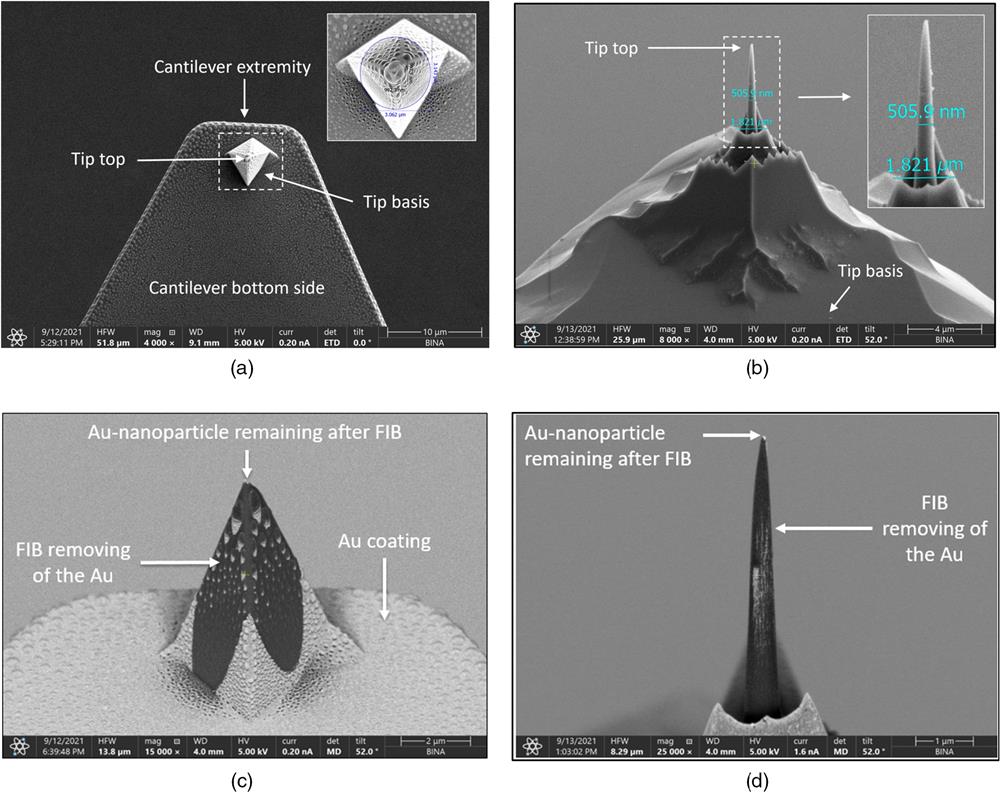
    Fig. 1. SEM micrographs of the commercial AFM probes before and after custom processing: (a) NP-S10 probe (bottom view); (b) TESP-HAR probe (side view); (c) NP-S10 probe after Au thin-film deposition and subsequent FIB processing; FIB removal of the Au thin film can be observed; (d) TESP-HAR probe after Au thin-film deposition and subsequent FIB processing.
    (a) SEM image of the custom-modified probe (NP-S10): AFM silicon tip with an Au NP at its apex. One can assume a circular shape of this NP, with radius R. Diagram of (b) half-sphere and (c) thin cylinder models by which the NP can be approximated.
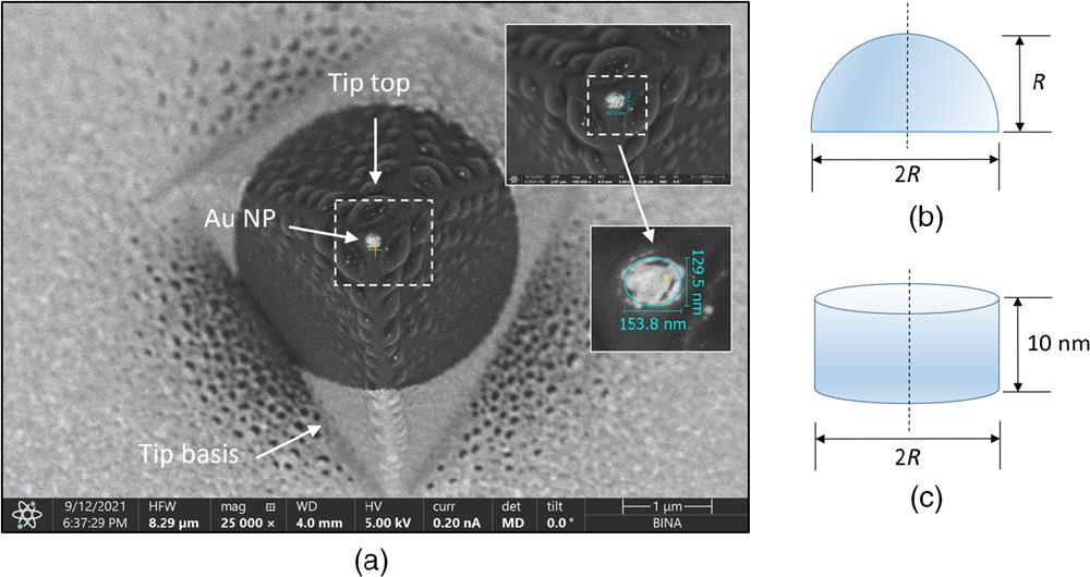
    Fig. 2. (a) SEM image of the custom-modified probe (NP-S10): AFM silicon tip with an Au NP at its apex. One can assume a circular shape of this NP, with radius R. Diagram of (b) half-sphere and (c) thin cylinder models by which the NP can be approximated.
    COMSOL geometry models: (a) 2D layers and (b) 3D layers concepts for the half-sphere model. The geometry is divided in three layers: PML, air, and Au NP. In this specific case, the illumination of the sphere is considered along the x axis, while the relative electric field is along the z axis.
    Fig. 3. COMSOL geometry models: (a) 2D layers and (b) 3D layers concepts for the half-sphere model. The geometry is divided in three layers: PML, air, and Au NP. In this specific case, the illumination of the sphere is considered along the x axis, while the relative electric field is along the z axis.
    Characterization workflow: (a) SEM analysis of the NP at the top of the tip; (b) cantilever extremity under dark-field; (c) spectra under bright and dark-field modes; and (d) experimental system configuration. Incident white light illuminates the optically resolved tip. The tip extremity is then observed using a dark-field objective lens, so the scattered light is filtered and observed. The scattered light is then split into two paths: the first one is used for optical imaging through the camera, and the second one is used for spectrometry analysis aimed at detecting the positions of the resonance peaks.
    Fig. 4. Characterization workflow: (a) SEM analysis of the NP at the top of the tip; (b) cantilever extremity under dark-field; (c) spectra under bright and dark-field modes; and (d) experimental system configuration. Incident white light illuminates the optically resolved tip. The tip extremity is then observed using a dark-field objective lens, so the scattered light is filtered and observed. The scattered light is then split into two paths: the first one is used for optical imaging through the camera, and the second one is used for spectrometry analysis aimed at detecting the positions of the resonance peaks.
    SEM pictures of the custom-modified tips. Au NPs can be observed on the apex of the probes. (a) NP-S10 probe; (b) TESP-HAR probe; (c) top view of the diameters starting from the basis of the tip (μm) and up toward upper stages of the tip (nm); and (d) zoom-in of the top view. Dimensions of the Au NPs are presented in (a) and (b).
    Fig. 5. SEM pictures of the custom-modified tips. Au NPs can be observed on the apex of the probes. (a) NP-S10 probe; (b) TESP-HAR probe; (c) top view of the diameters starting from the basis of the tip (μm) and up toward upper stages of the tip (nm); and (d) zoom-in of the top view. Dimensions of the Au NPs are presented in (a) and (b).
    COMSOL results on the scattering and absorption cross sections using the half-sphere model. For NPs of different radii deposited on the apex of the NP-S10 probe: graphs of the (a) scattering and (b) absorption. For NPs of different radii deposited on the apex of the TESP-HAR based tip: graphs of the (c) scattering and (d) absorption.
    Fig. 6. COMSOL results on the scattering and absorption cross sections using the half-sphere model. For NPs of different radii deposited on the apex of the NP-S10 probe: graphs of the (a) scattering and (b) absorption. For NPs of different radii deposited on the apex of the TESP-HAR based tip: graphs of the (c) scattering and (d) absorption.
    COMSOL results on the scattering and absorption cross sections using the cylinder model. For NPs of different radii deposited on the apex of the NP-S10 probe: graphs of the (a) scattering and (b) absorption. Since for NPs with radii of 70 and 75 nm, the curves are fully matched; we present only the results for the 75 nm NP. For NPs of different radii deposited on the apex of the NP-S10 TESP-HAR probe: graphs of the (c) scattering and (d) absorption.
    Fig. 7. COMSOL results on the scattering and absorption cross sections using the cylinder model. For NPs of different radii deposited on the apex of the NP-S10 probe: graphs of the (a) scattering and (b) absorption. Since for NPs with radii of 70 and 75 nm, the curves are fully matched; we present only the results for the 75 nm NP. For NPs of different radii deposited on the apex of the NP-S10 TESP-HAR probe: graphs of the (c) scattering and (d) absorption.
    Spectrometer measurements of the resonance wavelength. (a) Bright-field mode, magnification M=150×, and integration time t=900 ms. (b) Dark-field mode, magnification M=50×, and integration time t=900 ms. (c) Comparison of bright field, dark field, and reference spectra.
    Fig. 8. Spectrometer measurements of the resonance wavelength. (a) Bright-field mode, magnification M=150×, and integration time t=900  ms. (b) Dark-field mode, magnification M=50×, and integration time t=900  ms. (c) Comparison of bright field, dark field, and reference spectra.
    Validation of AFM function by comparing the tapping-mode topographic outputs of the processed TESP-HAR-Au tip versus the commercial nonprocessed TESP-HAR tip. AFM imaging of (a) VGRP-15M platinum (Pt)-coated reference sample, (b) series of Au spherical NPs, and (c) single Au spherical NP. Topography curves along the white profile line for (d) VGRP-15M platinum (Pt)-coated reference sample, (e) series of Au spherical NPs, and (f) single Au spherical NP. Scan comparison results on (g) VGRP-15M sample, (h) spherical NPs sample, and (i) single spherical NP sample.
    Fig. 9. Validation of AFM function by comparing the tapping-mode topographic outputs of the processed TESP-HAR-Au tip versus the commercial nonprocessed TESP-HAR tip. AFM imaging of (a) VGRP-15M platinum (Pt)-coated reference sample, (b) series of Au spherical NPs, and (c) single Au spherical NP. Topography curves along the white profile line for (d) VGRP-15M platinum (Pt)-coated reference sample, (e) series of Au spherical NPs, and (f) single Au spherical NP. Scan comparison results on (g) VGRP-15M sample, (h) spherical NPs sample, and (i) single spherical NP sample.
    (a) Conventional tip-enhanced fluorescence (left) versus tip-enhanced fluorescence based on PRET (right). In conventional TEF, the optical properties of the tip are not considered, and the excitation (λf-ex) is tuned to the maximum of the absorption band of the fluorescent molecule of interest. With PRET-based TEF, the laser beam used for excitation (λp-ex) matches the plasmon band of the tip, and fluorescence is obtained by dual effect, direct illumination, and PRET from tip (donor) to sample (acceptor), thus reducing the background and yielding higher SNR. (b) Condition for the PRET effect to take place. The plasmon resonance band overlaps with the fluorophore absorption band. When the plasmon band is positioned on the left tail of the absorption spectrum, the excitation light has a low contribution on the emission of illuminated fluorophores not benefiting from the PRET effect (those positioned far from the tip). Conversely, fluorophores under the tip would exhibit stronger emission due to the dual PRET and direct excitation effects.
    Fig. 10. (a) Conventional tip-enhanced fluorescence (left) versus tip-enhanced fluorescence based on PRET (right). In conventional TEF, the optical properties of the tip are not considered, and the excitation (λf-ex) is tuned to the maximum of the absorption band of the fluorescent molecule of interest. With PRET-based TEF, the laser beam used for excitation (λp-ex) matches the plasmon band of the tip, and fluorescence is obtained by dual effect, direct illumination, and PRET from tip (donor) to sample (acceptor), thus reducing the background and yielding higher SNR. (b) Condition for the PRET effect to take place. The plasmon resonance band overlaps with the fluorophore absorption band. When the plasmon band is positioned on the left tail of the absorption spectrum, the excitation light has a low contribution on the emission of illuminated fluorophores not benefiting from the PRET effect (those positioned far from the tip). Conversely, fluorophores under the tip would exhibit stronger emission due to the dual PRET and direct excitation effects.
    Radius (nm)30354070758090
    Scattering (nm)522524526555565575590
    Absorption (nm)512512514514508502500
    Table 1. Wavelengths of the maximum scattering and absorption for Au NPs with radii of different sizes, calculated by approximating the tip shape with the half-sphere model.
    Radius (nm)303540758090
    Scattering (nm)530532534522530524
    Absorption (nm)518516508500504502
    Table 2. Wavelengths of the maximum scattering and absorption for Au NPs with radii of different sizes, calculated by approximating the tip shape with the cylinder model.
    Jeremy Belhassen, Simcha Glass, Eti Teblum, George A. Stanciu, Denis E. Tranca, Zeev Zalevsky, Stefan G. Stanciu, Avi Karsenty. Toward augmenting tip-enhanced nanoscopy with optically resolved scanning probe tips[J]. Advanced Photonics Nexus, 2023, 2(2): 026002
    Download Citation