
Jeremy Belhassen, Simcha Glass, Eti Teblum, George A. Stanciu, Denis E. Tranca, Zeev Zalevsky, Stefan G. Stanciu, Avi Karsenty. Toward augmenting tip-enhanced nanoscopy with optically resolved scanning probe tips[J]. Advanced Photonics Nexus, 2023, 2(2): 026002
- Advanced Photonics Nexus
- Vol. 2, Issue 2, 026002 (2023)
Abstract
1 Introduction
Chemical and structural imaging with nanoresolution under ambient conditions is of the utmost importance for advancing our knowledge on biological processes occurring at the subcellular level,1
Another family of techniques, based on tip-enhanced optical effects, has emerged over the past years as a valuable alternative that can successfully overcome the above-mentioned limitations of f-SRM. Techniques belonging to this family, such as scattering-type scanning near-field optical microscopy (s-SNOM),14 tip-enhanced Raman spectroscopy (TERS),15 tip-enhanced fluorescence (TEF),16 second-harmonic generation scanning near-field optical microscopy (SHG-SNOM),17,18 tip-enhanced photoluminescence,19 and photoinduced force microscopy (PiFM),20 have gained tremendous interest, as they can obtain optical information at nanoscale resolution, limited only by the size of the tip used for scanning the sample, irrespective of the wavelength used for excitation.21 Other important features of these techniques are their ability to be used in ambient conditions, as well as their use under very low-power excitation conditions, which are not harmful to the investigated samples. Landmark experiments have shown that these techniques can be harnessed to yield resolutions, even below 1 nm.19,22 A major advantage of these techniques is that they share an important overlap in their architecture; they all rely on the illumination of a sharp, atomic force microscopy (AFM)-like, probe (also known as tip) that scans the surface of the sample, and on the subsequent detection of optical signals associated with the light–probe interaction. Such overlap facilitates correlative use, which is highly useful for experiments that require in-tandem access to complementary information that can be provided by such techniques.23
The contrast mechanisms of s-SNOM enable mapping the dielectric properties28
Sign up for Advanced Photonics Nexus TOC. Get the latest issue of Advanced Photonics Nexus delivered right to you!Sign up now
Although the field of TEN is constantly expanding, most imaging and spectroscopy applications reported to date rely on commercial scanning probes that are not specifically developed for TEN, but rather for AFM14,81,82 or for various other types of nonoptical scanning probe microscopy techniques. A consequence of this is that the optical properties of these tips are not provided by the manufacturers, as they are irrelevant to the applications they natively target. This issue is exacerbated by the fact that important properties, such as absorption, scattering, and reflectance are difficult to experimentally measure for objects at the scale of scanning probe tips. In this work, we propose an approach for TEN, where techniques such as those mentioned above, harness the versatility, potential, and performance of tips that are specifically designed and manufactured for applications in nanoscale tip-enhanced optical imaging. To this end, we propose a framework based on COMSOL simulations83 and nanomanufacturing that represents a solution for developing specialized tips for TEN, with well-understood and tailorable optical properties. This follows up on recent related endeavors, which have demonstrated the very high potential of TEN imaging with application customized probes.19,84 We provide a proof-of-concept example, in which we design and fabricate two variants of silicon scanning probe tips featuring Au NPs on their apex, whose optical properties we approximate by numerical simulations. Although previous efforts successfully demonstrated, in the context of other applications, scanning probe tips with various attached NPs,85
2 Methods
2.1 Tip-Fabrication Methodology
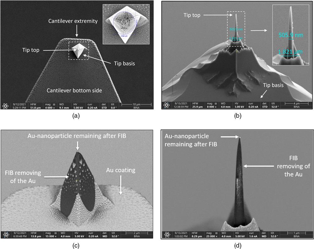
Two custom-modified probes were fabricated, based on commercially available ones. We opted for silicon probes that do not present plasmon effects overlapping with those of the plasmonically active material that we employed (Au). Using such probes as foundation for this framework results in a simple and reproducible fabrication process. In Fig. 1, scanning electron microscope (SEM) pictures of the two AFM tips, NP-S10 (Bruker) [Fig. 1(a)] and TESP-HAR (Bruker) [Fig. 1(b)], can be observed. These were modified in two steps [Figs. 1(c) and 1(d)] so that an Au NP is positioned on their apex. The tips were first coated with a 10-nm-thick Au layer by sputter deposition. Afterward, the Au layer was removed by focused ion beam (FIB)88,89 sputtering over the whole tip excepting the apex, resulting in an Au nanoparticle (NP) remaining there. In Figs. 1(c) and 1(d), one can observe the last step of the tip fabrication.
![]()
Figure 1.SEM micrographs of the commercial AFM probes before and after custom processing: (a) NP-S10 probe (bottom view); (b) TESP-HAR probe (side view); (c) NP-S10 probe after Au thin-film deposition and subsequent FIB processing; FIB removal of the Au thin film can be observed; (d) TESP-HAR probe after Au thin-film deposition and subsequent FIB processing.
2.2 COMSOL Simulations Methodology
2.2.1 Half-sphere and cylinder models
The physical parameters of interest in this experiment are the probe’s plasmon band and its size. Although experimental measurements of the scattering and absorption spectrum of the probe could potentially be used to assess its plasmon band, such results are very difficult to obtain on nanosized objects. However, numerical analysis does not suffer from this limitation. Moreover, as recently shown in other works on TEN imaging, simulation methods allow for the testing of different tip geometries and sizes so as to identify their influence on the imaging outputs.90 As discussed further in this section, to fabricate TEN probes with known optical properties, we adopted a fabrication approach whose final result is the deposition of an Au NP of custom size on the apex of a commercial AFM probe. Two commercial AFM probes with distinct geometries were considered, NP-S10 (Bruker) and TESP-HAR (Bruker).
In Fig. 2(a), an SEM image of the apex of one of the custom-modified probes is presented, with the Au NP clearly noticeable at the extremity of the tip. Since we have used a probe substrate (Si) that is plasmonically inactive in the spectral region matching the plasmon band of the Au NP, any potential plasmon resonance energy transfer (PRET) occurring between the tip and the sample will be governed by the optical properties of the Au NP alone. It follows that it suffices to model only the NP in our COMSOL simulations. In addition, although the fabrication process discussed earlier results in an ellipsoidal-shaped NP, we assume that it can be accurately modeled as either a half-sphere [Fig. 2(b)] or a thin cylinder [Fig. 2(c)], both of radius .
![]()
Figure 2.(a) SEM image of the custom-modified probe (NP-S10): AFM silicon tip with an Au NP at its apex. One can assume a circular shape of this NP, with radius
The radii of the NP models used in the COMSOL simulations were determined by measurements performed on the actual particles after the fabrication procedure. The radii were found to lie in the following ranges.
The initial radii of curvature of the two considered probes were 20 and 10 nm for the NP-S10 and TESP-HAR probes, respectively.
2.2.2 Model implementation in COMSOL
In Fig. 3, we present the geometry of our COMSOL simulation for the case of the hemispherically approximated NP. Given the high computational time required for 3D finite-element method simulations, only half of the NP was modeled; symmetry lets us extrapolate the results to the entire structure. (This methodology was inspired by a COMSOL Applications Library example on Mie scattering that addressed structures of a similar kind.) One can discern three different layers in the representation of the model. The outer one is a perfectly matched layer (PML), used to simulate open boundaries91 by absorbing the outgoing electromagnetic waves and canceling spurious reflections; the middle one models the ambient air around the NP; and the inner one models the NP itself. The illumination is simulated as electromagnetic plane waves propagating along the axis. The measurement of the scattering and absorption was performed by integration over the entire external interface of the air layer. The simulation concept for the cylinder shape model is defined along similar lines.
Sign up for Advanced Photonics Nexus TOC. Get the latest issue of Advanced Photonics Nexus delivered right to you!Sign up now
![]()
Figure 3.COMSOL geometry models: (a) 2D layers and (b) 3D layers concepts for the half-sphere model. The geometry is divided in three layers: PML, air, and Au NP. In this specific case, the illumination of the sphere is considered along the
2.3 Resonance Characterization Methodology
To measure the effective plasmon resonance of the probes, a challenging series of measurements of the light spectrum scattered from the tip were performed by means of a spectrometer connected to fiber optics. The scattering from the tip was obtained via dark-field microscopy using a Carl Zeiss Axiotron optical microscope, and a ThorLabs Compact Spectrometer 350 to 700 nm was connected to the system and used for the resonance measurements. Figure 4 presents various images of the cantilever and tip characterization under bright- and dark-field microscopy. Figure 4 shows the experimental characterization system configuration. Figure 4(a) presents the fabricated NP on the top of the tip, using an SEM. By means of this configuration, spectra were obtained and compared for several intensities [Fig. 4(c)]. The last step consisted in a screening analysis in order to identify the plasmon resonance wavelength [Fig. 4(d)].
![]()
Figure 4.Characterization workflow: (a) SEM analysis of the NP at the top of the tip; (b) cantilever extremity under dark-field; (c) spectra under bright and dark-field modes; and (d) experimental system configuration. Incident white light illuminates the optically resolved tip. The tip extremity is then observed using a dark-field objective lens, so the scattered light is filtered and observed. The scattered light is then split into two paths: the first one is used for optical imaging through the camera, and the second one is used for spectrometry analysis aimed at detecting the positions of the resonance peaks.
2.4 Description of the Setup Used for Validating the AFM Function of the Processed Probes
Atomic force microscopy (AFM) measurements were carried out using a Bio FastScan scanning probe microscope (Bruker AXS). All images were obtained under tapping mode operation with the nonprocessed TESP-HAR and processed TESP-HAR-Au probes. The measurements were performed under environmental conditions in an acoustic hood to minimize the vibrational noise. The images were captured in the retrace direction with a scan rate of 1.0 Hz. The resolution of the images was 256 samples/line. For the image processing and analysis, we used Nanoscope Analysis software. The “flatting” and “planefit” functions were applied to each image.
3 Results
3.1 Au Apex Shapes and Measured Dimensions
As discussed in the introduction, the purpose of this experiment is to demonstrate the viability of combining nanofabrication and numerical simulation in the manufacture of custom TEN probes. We previously detailed the two-stage process through which commercial grade probes were modified to equip their apex with Au NPs (first sputter deposition and then FIB removal); here we present the results of that process. One can observe the dimensions of the Au NPs that resulted for the NP-S10 and TESP-HAR probes in Figs. 5(a) and 5(b), respectively. For the NP-S10 probe, the smallest NP obtained (dictated by the maximum FIB resolution) was of ellipsoidal shape, with axes of 129.5 and 153.8 nm, and therefore, an eccentricity of 0.54. For the TESP-HAR probe, the smallest Au NP obtained was also of ellipsoidal shape, with axes of 70.15 and 75.54 nm and an eccentricity of 0.27. Figures 5(c) and 5(d) present top views of the different existing diameters from the bottom of the tip to its top.
![]()
Figure 5.SEM pictures of the custom-modified tips. Au NPs can be observed on the apex of the probes. (a) NP-S10 probe; (b) TESP-HAR probe; (c) top view of the diameters starting from the basis of the tip (
3.2 Numerical Results
3.2.1 COMSOL simulation results for the half-sphere model
In Fig. 6, we present our simulations of the scattering [Figs. 6(a) and 6(c)] and absorption [Figs. 6(b) and 6(d)] cross sections as a function of the wavelength for the half-sphere model. Different radii (Fig. 2) were simulated in a range of sizes close to the dimensions of the fabricated tips. Since in reality the NP exhibits an ellipsoidal shape, the radii tested were chosen to be in the range between the sizes of the semiminor and semimajor axes. We assume that the properties of the real tips are close in value to the results numerically simulated for the considered range of . Table 1 shows the value of the scattering and absorption cross sections’ maxima as a function of the radius.
![]()
Figure 6.COMSOL results on the scattering and absorption cross sections using the half-sphere model. For NPs of different radii deposited on the apex of the NP-S10 probe: graphs of the (a) scattering and (b) absorption. For NPs of different radii deposited on the apex of the TESP-HAR based tip: graphs of the (c) scattering and (d) absorption.
| Radius (nm) | 30 | 35 | 40 | 70 | 75 | 80 | 90 |
| Scattering (nm) | 522 | 524 | 526 | 555 | 565 | 575 | 590 |
| Absorption (nm) | 512 | 512 | 514 | 514 | 508 | 502 | 500 |
Table 1. Wavelengths of the maximum scattering and absorption for Au NPs with radii of different sizes, calculated by approximating the tip shape with the half-sphere model.
For a radius , corresponding to the ellipsoidal NP of the NPS-10, one can observe the following. First, for all the considered radii, a local maximum of the scattering is observed between 555 and 590 nm (see also Table 1). These values are close to 532 and 561 nm, two wavelengths that are commonly used for fluorescence microscopy,92,93 an aspect that can potentially be used in TEF applications building on PRET. Second, the wavelength corresponding to the resonance of the scattering increases with the NP radius. Concerning the absorption cross section, for all the different radii, the maxima are observed between 500 and 514 nm (see Table 1). In Figs. 6(c) and 6(d), we present the simulated scattering and absorption cross sections, respectively, for the considered radii range corresponding to the ellipsoidal NP of the TESP-HAR probe. The scattering cross sections’ maxima were obtained in the range from 522 to 526 nm, whereas the absorption cross sections’ maxima were obtained in the range from 512 to 514 nm.
According to the quasistatic approximation, the scattering and absorption maxima have to match. The corresponding scattering and absorption cross sections of a sphere of radius , calculated via the Poynting vector, from the full electromagnetic (EM) field associated with an oscillating dipole are defined by the following set of equations.94 The expression of the scattering cross section is given by the following equation:
The resonance is obtained at the Fröhlich condition [Eq. (4)],
In case of a large NP, the corresponding scattering and absorption cross sections will become Eqs. (5) and (6), respectively,
3.2.2 COMSOL simulation results for the cylinder model
In Fig. 7, we present the simulated scattering and absorption cross sections as a function of the wavelength for the cylinder model. For a radius corresponding to the ellipsoidal NP of the NPS-10, the following phenomena can be observed for the scattering [Fig. 7(a)] and absorption [Fig. 7(b)] cross sections: first, for all the different radii, a local maximum of the scattering phenomenon is observed between 522 and 530 nm. However, contrary to the half-sphere model results, one can notice that the wavelength corresponding to the resonance of the scattering seems here to decrease with the radius. In regard to the absorption cross section, for all the different radii, the maxima are observed between 500 and 504 nm. The scattering and absorption cross section results for the NP deposited on the apex of the TESP-HAR are presented in Figs. 7(c) and 7(d), respectively. In this case, the maxima of the scattering cross sections are localized between 530 and 534 nm, whereas the absorbtion cross sections’ maxima are localized between 508 and 518 nm. The value of the scattering and absorption cross sections’ maxima is summarized in Table 2 as a function of the NP radius.
![]()
Figure 7.COMSOL results on the scattering and absorption cross sections using the cylinder model. For NPs of different radii deposited on the apex of the NP-S10 probe: graphs of the (a) scattering and (b) absorption. Since for NPs with radii of 70 and 75 nm, the curves are fully matched; we present only the results for the 75 nm NP. For NPs of different radii deposited on the apex of the NP-S10 TESP-HAR probe: graphs of the (c) scattering and (d) absorption.
| Radius (nm) | 30 | 35 | 40 | 75 | 80 | 90 |
| Scattering (nm) | 530 | 532 | 534 | 522 | 530 | 524 |
| Absorption (nm) | 518 | 516 | 508 | 500 | 504 | 502 |
Table 2. Wavelengths of the maximum scattering and absorption for Au NPs with radii of different sizes, calculated by approximating the tip shape with the cylinder model.
3.3 Characterization Results
3.3.1 Bright field versus dark field
To enable clear identification of the plasmon response, after checking the tip in bright-field mode [Fig. 4(a)], it was necessary to illuminate the cantilever and the tip in dark-field mode [Figs. 4(b) and 4(c)]. Several challenges arose in the effort to illuminate the tip. First, even if the illumination is off, the background illumination resulting from the scattering due to the edges of the silicon cantilever still has influence on the spectrum. Thus, while trying to isolate the resonance peak from the extremity of the Au NP, one can assume that the additional spectral responses are obtained from the rest of the probe, also covered by a metal layer. This is why it is not straightforward to measure the optical properties of individual small objects placed in proximity of other structures, and some gaps may appear compared to the simulations, where one can isolate an illuminated surface with high accuracy, and the measured spectrum obtained through the whole system.
3.3.2 Spectrometer curves
Although numerical results (also known as COMSOL simulations) presented a forecast of the tips’ expected behavior, experimental results became necessary to confirm and analyze the scattering and the absorption phenomena. As per previous works, based on Mie theory, it appeared that for highly doped Si NPs (known to act as a metal), the resonance frequency increases with the size of the NP.99 Similar conclusions were obtained with silver NPs sharing different sizes.100 Dark-field optical microscopy can be used to detect plasmon resonance of a single particle, since the dark-field condenser acts like a filter for the directly transmitted light, whereas only the scattered light is observed.94 Since plasmon resonance leads to scattering maximum [Eqs. (1) and (5)], the effect of incident white light is studied to find in which visible wavelength the resonance occurs. The scattered light is then analyzed by spectrometry analysis. Figure 8 presents a series of measured spectra, recorded while illuminating the tips in bright- and dark-field modes. At this stage, it appeared that the most promising type of tip, toward future optically resolved scanning probes, was the TESP-HAR model, given the higher consistency of the obtained results. Indeed, the resonance wavelength, obtained by the performed simulation, matches the common 532 nm illumination wavelength, which can be desired in practical applications (as shown in Fig. 7 and Table 2). Regarding the fabricated probes, Fig. 8(a) presents the measured spectrum in bright-field mode. A resonance peak can be observed at 538 nm. Figure 8(b) presents the measured spectrum in dark-field mode. Although dimmer, the resonance peak at 538 nm can still be observed. It should be noted that the measured intensity in the dark-field mode is almost one-third when compared to the bright-field mode’s intensity, for the same integration time of 900 ms.
![]()
Figure 8.Spectrometer measurements of the resonance wavelength. (a) Bright-field mode, magnification
3.4 Validation of AFM Function of the Processed Tips
Although showcasing advantages of the proposed tips and of the associated optical modeling framework will be addressed in dedicated follow-up work, we present next a series of results that demonstrate the unaltered AFM function of the processed probes.
To demonstrate the unaltered capabilities for topographic imaging of the modified probes, we performed tapping-mode AFM on several types of samples, such as nanoantenna and nanospheres with the commercial, nonprocessed, TESP-HAR probes and with the modified instances, TESP-HAR-Au. Similar results (not shown here) were obtained for the NP-S10 probes. Figure 9 presents the main results of the scanning experiments performed on the following.
![]()
Figure 9.Validation of AFM function by comparing the tapping-mode topographic outputs of the processed TESP-HAR-Au tip versus the commercial nonprocessed TESP-HAR tip. AFM imaging of (a) VGRP-15M platinum (Pt)-coated reference sample, (b) series of Au spherical NPs, and (c) single Au spherical NP. Topography curves along the white profile line for (d) VGRP-15M platinum (Pt)-coated reference sample, (e) series of Au spherical NPs, and (f) single Au spherical NP. Scan comparison results on (g) VGRP-15M sample, (h) spherical NPs sample, and (i) single spherical NP sample.
The unaltered AFM function of the processed tips can be best observed based on the three topographic profiles recorded with both nonprocessed and processed tips, TESP-HAR and TESP-HAR-Au. Although tiny amplitude and phase shifts between the two measured curves are noticeable, the results obtained for both tips are similar, which means that in spite of the processing the TESP-HAR-Au maintains its AFM capability. The differences between the curves can be explained by several aspects that do not affect the validity of the successful concept. First, the addition of an NP at the end of a tip can affect the diameter of its apex. By processing according to the proposed methodology, the diameter of a commercial AFM tip will increase by few tens of nanometers. Such a change will not affect the accuracy on long scans, as presented in Figs. 9(g) and 9(h), where the amplitudes are similar for both TESP-HAR and TESP-HAR-Au. However, it can affect the scans of objects of smaller dimensions, as presented in Fig. 9(i). An additional explanation of the noticeable phase shifts is purely related to a small registration mismatch between the positions of the profile lines with respect to the sample surface. This experiment has been done manually and bringing the two scan curves on the same graph was intended for proof-of-concept comparison, to show that the processed tip kept its capability to scan; therefore, precise and nanometer-level registration was not intended.
4 Discussion
At present, although TEN imaging has enabled important discoveries, the outputs of these techniques are largely biased by the use of nonspecialized probes. Here we propose the idea of using optically resolved probes, which can potentially significantly augment nanoscale imaging with TEN, by enabling routes for a higher SNR, and consequently, higher resolution and faster acquisition rates. We showed that by coating a commercial AFM probe with a thin layer of Au, and then processing it by FIB, an Au NP can be placed on its apex. By experimenting with two very different probes, we demonstrated that this methodology can be implemented irrespective of the tip’s geometry. Other materials besides Au, such as Pt, Cr, and Ag, could also be used, depending on the tip properties required by specific applications. Alternative approaches, not demonstrated here, could consist in attaching NPs of known size and shape to tipless cantilevers, but according to our past experiences on the topic, such approaches can be significantly more challenging. Furthermore, such approaches would result in probes with peculiar tip-shanks, whereas the current body of understanding on near-field data90 incorporates the specific geometries of traditional AFM tips, which the methodology proposed here better maintains. Further on, we showed that by COMSOL numerical simulations we can approximate the optical properties of the NP resulting on the probe apex after FIB processing. Experimental assays based on bright-field and dark-field microscopy and spectroscopy can be eventually implemented to validate the numerical results. We consider that the proposed framework could result in the advent of TEN imaging approaches where investigations are done with specialized tips whose known optical properties can be exploited for better and faster investigations. To this end, in the next paragraph, we discuss two potential applications.
TEF implementations that rely on the coupling between the absorption band of fluorophore and localized surface plasmon resonance of the tip-substrate system,16,101,102 hold important potential to resolve many of the typical drawbacks of more simplistic TEF imaging approaches, where the properties of the probe are not thoroughly taken into account,74
![]()
Figure 10.(a) Conventional tip-enhanced fluorescence (left) versus tip-enhanced fluorescence based on PRET (right). In conventional TEF, the optical properties of the tip are not considered, and the excitation (
The following question naturally arises: would investigations on distinct fluorophores, with different absorption bands, require the use of different tips, each with a plasmon band matching the absorption band of the fluorophore in question? We speculate that this can potentially be avoided by implementing clever strategies where the absorption/plasmon band of the tip can be tuned. Such a potential strategy can eventually rely on previous work showing that submicrometer particle-based structures can be employed to reconfigure photonic devices by external photonic radiation. One of the device configurations that was previously demonstrated involved metallic NPs or nanorods incorporated into a semiconducting structured matrix that exhibits strong plasmonic resonance, which depends on the power of the external photonic radiation that is being absorbed by the matrix.104 Taking inspiration from this previous work, future specialized TEN probes can be designed to feature optical tunability obtained by adding an external control beam that, when absorbed in a silicon part of the tip nanostructure, will produce free electrons, leading to tuning of the plasmonic resonance of the nanostructure at the end of the tip, thus improving the energy transfer process by properly matching the plasmonic resonance to the plasmonic excitation wavelength. Given that such tips will possess a tunable plasmon band, the same tip will be capable of imaging various fluorescent molecules. In addition to its use for fluorescence imaging, this strategy could also enable subnanometer imaging of nonfluorescent materials.
On a different train of thought, we refer to probably the most well-known TEN technique, s-SNOM. The working principles of s-SNOM rely on a sharp tip that is scanned across the sample’s surface while it is being excited with a focused laser beam. The attainable resolution in s-SNOM depends on the size and geometry of the probe, with many important applications having been reported for tip sizes ranging between 5 and 150 nm.82,91,105,106 The tip converts the incident radiation into a highly localized and enhanced near field at the tip apex, which modifies both the amplitude and the phase of the scattered light via the near-field interaction with the sample underneath.14 This process depends on the local dielectric properties of the tip and sample. The default way of extracting s-SNOM signals is by lock-in detection of the optical signals corresponding to the tip–sample interaction, which are modulated by the tapping movement of the tip.14 We speculate that this type of modulation, achieved by mechanical means, can be replaced, or augmented with an alternative/additional modulation scheme, by means of a pump beam tuned to the plasmon band of the tip, which can intermittently plasmonically activate/deactivate the tip, at ultrafast rates, and depending on the properties of the sample, it can modify the interaction of the two mirror dipoles (in probe and sample) accounting for s-SNOM contrast.107,108 This pump beam would complement the probe beam, which in many s-SNOM applications is tuned to the absorption band of the sample to promote phase contrast.14,43,81,109 An additional layer of (faster) modulation can eventually provide higher SNR. Furthermore, this alternative modulation scheme based on on–off switching of the pump beam could even entirely replace the traditional modulation schemes based on the tapping movement of the probe, which could enable s-SNOM imaging in contact mode, which would be faster than tapping-mode s-SNOM (which is the current default way of performing s-SNOM investigations), and more suited for some applications, depending on the sample type and scanning environment. In addition to considering the tip’s absorption as the key for signal modulation, referring to its scattering can also represent a route. For example, by intermittently using two close wavelengths, accounting for significantly different scattering-levels from the tip, we speculate that the s-SNOM signals can be modulated as well. Similar modulation approaches can eventually be implemented for other TEN modalities, such as TERS and PiFM. Overall, we consider that having at hand probes with precisely known optical properties can open an entire new palette of data acquisition strategies for TEN techniques that can enable better outputs in terms of signal quality, sensitivity, robustness, and speed. Future work refining this technology from the plasmon coupling perspective110 will be important.
In addition to imaging, the interaction between focused light and AFM probes was also demonstrated in highly useful nanolithography and ablation purposes.97,98,111 We argue that in such applications, the use of optically resolved probes can also be important in optimizing the outputs, as the interactions between tip and sample are likely to be entirely different for situations when the illumination wavelength matches or not the absorption or scattering of the tip. Furthermore, these properties can potentially also be correlated with the heating profiles of the tip, which were previously shown to have an important impact over the final outputs of tip-enhanced nanoablation.112
Finally, we turn our attention to the issue of attainable resolution. Although the results presented here do not align, in terms of tip size, to the state-of-the art on AFM probe sharpness, the motivation behind this proof-of-concept experiment was not aimed at addressing this particular problem. We speculate that adjusting our proposed methodology to incorporate the use of probes with different geometries, in combination with different processing methods, can eventually result in sharper probes. However, we find noteworthy to recall recent results,82 which show that tip sharpness is not always preferred. Thus we consider that having a precise understanding of the tip’s optical properties can at times be the better option to consider.
5 Conclusions
Tip-enhanced nanoscopies have enabled so far a wide palette of discoveries and account for new scientific breakthroughs each day. However, they rely on nonspecialized probes, usually designed and commercialized for various nonoptical scanning probe microscopy variants, which significantly biases their potential. Here we propose the concept of TEN probes with known optical properties. To this end, we custom modified two commercial AFM probes to equip their apex with an NP, whose absorption and scattering properties we approximated by numerical simulations in COMSOL, based on Mie scattering.113,114 We argue that the so-developed probes, with resolved optical properties, can enable various data acquisition schemes for faster and more sensitive TEN imaging and may also prove useful for nanolithography. A series of perspectives in this regard are discussed. Overall, we consider the reported framework to be highly flexible, allowing the design and fabrication of a wide range of tips with custom-tailorable optical properties exhibiting various geometries and material compositions.
Jeremy Belhassen received his BSc degree in physics in 2016 and his MSc degree in fundamental physics in 2019 from the Université Grenoble-Alpes, France, with a specialization in photonics/semiconductors with Phelma partnership. His MSc thesis was an international exchange with Jerusalem College of Technology (JCT). He is a PhD candidate at Bar-Ilan-University and JCT, under the joint supervision of Prof. Zeev Zalevsky and Dr. Avi Karsenty, and a research assistant at the Advanced Laboratory of Electro-Optics (ALEO) of JCT, working on nanophotonics/nanoelectronics devices development.
Simi Glass is a BSc student in electrical engineering at JCT, with a specialization in power supplies. He won the first place in the 2022 Israel Electric Corporation Student Contest, as part of the JCT team. He is a research assistant at the ALEO of JCT, under the supervision of Dr. Avi Karsenty, and is currently working on various projects involving micro/nanoscale material conductivity.
Eti Teblum received her PhD from Bar-Ilan University, Israel, in 2009. Her research experience includes polymers, organic chemistry synthesis, and materials science. She specialized in synthesizing 1D materials as CNT and CNF, and 2D materials as graphene and TMDs, by CVD and wet chemistry. In 2017, she joined BINA as an AFM export. Currently, she is BINA’s project manager and continues to operate the AFM unit at BINA. She has authored 34 scientific papers.
George A. Stanciu is a professor of physics at the University Politehnica of Bucharest. He received the Professor title in 1994. Since 1973, he has been working in the laser scanning microscopy field. His team reported the first digital laser scanning microscope. He is the head of the Center for Microscopy-Microanalysis and Information Processing. Lately, he is focused on different scanning laser microscopy techniques: instrumentation and applications. He is a senior member of the IEEE from 1995.
Denis-Emanuil Tranca has graduated the Faculty of Electronics, Telecommunications and Information Technology at the University Politehnica of Bucharest in 2010 and received his master’s degree in diploma in the field of optoelectronics from the same university two years later. In 2015, he defended his PhD thesis that was dealing with new detection and investigation applications for scattering scanning near-field optical microscopy. He has been involved in the research activities that take place at CMMIP-UPB since November 2011.
Zeev Zalevsky received his BSc and direct PhD degrees in electrical engineering from Tel-Aviv University in 1993 and 1996, respectively. He is currently a full professor and the dean of engineering at Bar-Ilan University, Israel. His major fields of research are optical super-resolution, biomedical optics, and nanophotonics. For his research, he received many national/international prizes and he is a fellow of many large scientific societies, SPIE, Optica, IEEE, EOS, NAI, and more.
Stefan G. Stanciu received his PhD in electronic engineering and is habilitated in physics. He currently acts as a senior researcher at the Center for Microscopy-Microanalysis and Information Processing of Politehnica University of Bucharest, being involved in research focusing, among others, on optical nanoscopy, biophotonics, advanced materials, and on AI-methods for high-resolution imaging. He has authored >70 WOS journal articles and currently serves as a senior editor for IEEE Photonics Journal and an associate editor for Frontiers in Photonics.
Avi Karsenty received his PhD in applied-physics/material-science (microelectronics/electro-optics divisions) from Hebrew University of Jerusalem Israel (HUJI) in 2003. He has more than two decades of experience in high-tech-industry in Europe and Israel, having spent years with Intel (1995 to 2011) in senior engineering/management. Back to academia (2011), he served as the head of the Applied-Physics/Electro-Optics Department (2014 to 2018) at JCT. He is an IEEE/Optica senior member, holding 40 awards in engineering/physics with >70 journal publications. He shares expertise in nanophotonics/nanoelectronics devices, quality and reliability, and super-resolution techniques. He leads the JCT Nanotechnology Center.
References
[3] L. Schermelleh et al. Super-resolution microscopy demystified. Nat. Cell Biol., 21, 72(2019).
[18] K. Yao et al. Nanoscale optical imaging of 2D semiconductor heterostructures by exciton enhanced second harmonic generation. Bull. Am. Phys. Soc., 67(2022).
[41] R. O. Freitas et al. Nano-infrared imaging of primary neurons. Cells, 10, 2559(2021).
[82] C. Maissen et al. Probes for ultrasensitive THz nanoscopy. ACS Photonics, 6, 1279-1288(2019).
[83] . Introduction to COMSOL Multiphysics®, 32(1998).
[84] T. Siday et al. Resonance-enhanced terahertz nanoscopy probes. ACS Photonics, 7, 596-601(2020).
[94] S. A. Maier. Plasmonics: Fundamentals and Applications(2007).
[103] S. G. Stanciu et al. A novel approach for near-field optical microscopy based on tip-enhanced fluorescence via plasmon resonance energy transfer (TEFPLASNOM), 1-6(2020).
[113] M. Fowler. AltaSim simulates Mie scattering of electromagnetic waves.
[114] J. Crompton, S. Yushanov, K. Koppenhoefer. Mie scattering of electromagnetic waves(2013).

Set citation alerts for the article
Please enter your email address
© Copyright 2018-2021 | Chinese Laser Press. All Rights Reserved 沪ICP备15018463号-20