• Photonics Research
  • Vol. 8, Issue 4, 519 (2020)
Wei Wang1, Fengping Yan1、*, Siyu Tan2, Haisu Li1, Xuemei Du1, Luna Zhang1, Zhuoya Bai1, Dan Cheng1, Hong Zhou3, and Yafei Hou4
Author Affiliations
  • 1Key Laboratory of All Optical Network & Advanced Telecommunication of EMC, Institute of Lightwave Technology, Beijing Jiaotong University, Beijing 100044, China
  • 2Zhengzhou Xinda Institute of Advanced Technology, Zhengzhou 450001, China
  • 3Department of Electronics, Information and Communication Engineering, Osaka Institute of Technology, 5-16-1 Omiya, Asahi-ku, Osaka, 535-8585, Japan
  • 4Graduate School of Natural Science and Technology, Okayama University, 1-1-1 Tsushimanaka, Kita Ward, Okayama Prefecture, 700-8530, Japan
  • show less
    DOI: 10.1364/PRJ.386040 Cite this Article Set citation alerts
    Wei Wang, Fengping Yan, Siyu Tan, Haisu Li, Xuemei Du, Luna Zhang, Zhuoya Bai, Dan Cheng, Hong Zhou, Yafei Hou. Enhancing sensing capacity of terahertz metamaterial absorbers with a surface-relief design[J]. Photonics Research, 2020, 8(4): 519 Copy Citation Text show less
    Schematic drawing shows the proposed process for fabricating an MA in detail. The processing steps are listed alphabetically. Different colors represent various materials, that is, light gray, purple, and green parts refer to the Si substrate, Al parts, and dielectric layer, respectively.
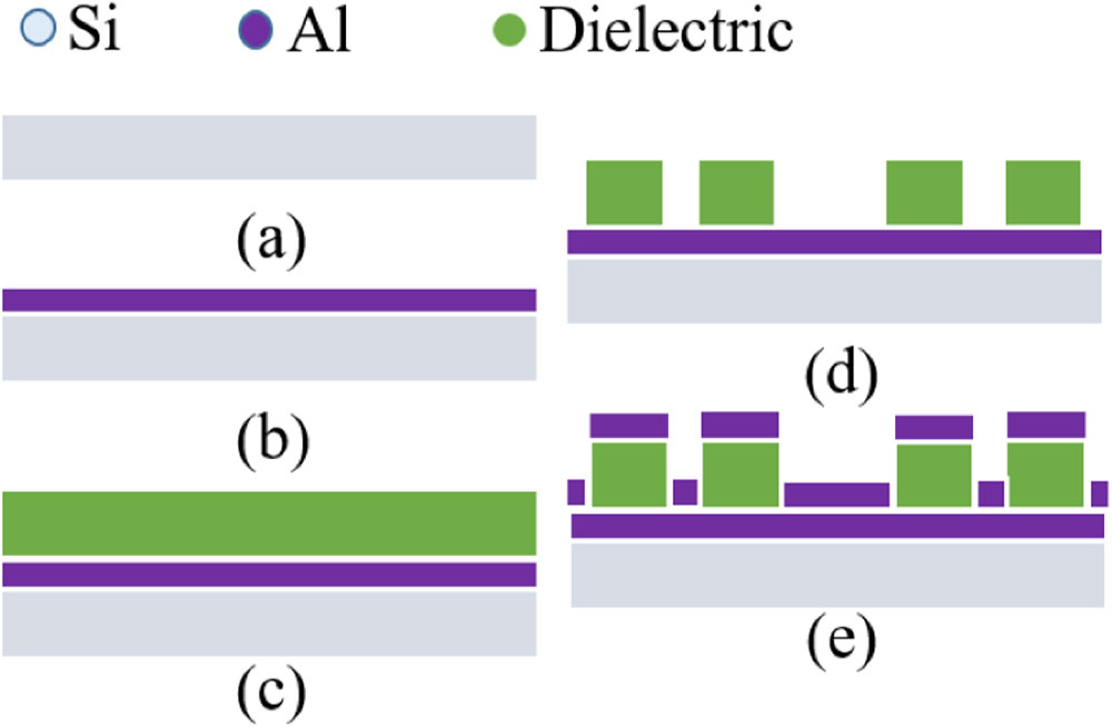
    Fig. 1. Schematic drawing shows the proposed process for fabricating an MA in detail. The processing steps are listed alphabetically. Different colors represent various materials, that is, light gray, purple, and green parts refer to the Si substrate, Al parts, and dielectric layer, respectively.
    3D schematic plot for the MA examples and the incident THz field polarizations. All the MAs are excited by the same incident field polarizations shown at the top right corner of the plot. Different colored parts represent different materials. (a) and (b) are the original and remolded (SR) cross-shaped MAs. (c) and (d) are the original and remolded (SR) square-shaped MAs. For all MAs, lattice constant, and thicknesses of metal and dielectric layers are labeled as p, t, and h, while l and w represent length and width of the metallic stripes constituting the cross and square structures in MAs, respectively.
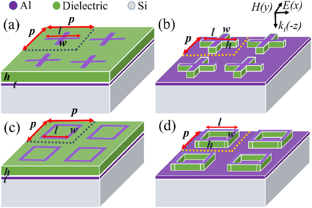
    Fig. 2. 3D schematic plot for the MA examples and the incident THz field polarizations. All the MAs are excited by the same incident field polarizations shown at the top right corner of the plot. Different colored parts represent different materials. (a) and (b) are the original and remolded (SR) cross-shaped MAs. (c) and (d) are the original and remolded (SR) square-shaped MAs. For all MAs, lattice constant, and thicknesses of metal and dielectric layers are labeled as p, t, and h, while l and w represent length and width of the metallic stripes constituting the cross and square structures in MAs, respectively.
    Comparison plots for absorption performance of two focused sets of MAs at the frequency band of 0.4 to 1.6 THz. (a) Cross MA versus SRC MA and (b) square MA versus SRS MA. The embedded tables show comparative information in a quantitative way.
    Fig. 3. Comparison plots for absorption performance of two focused sets of MAs at the frequency band of 0.4 to 1.6 THz. (a) Cross MA versus SRC MA and (b) square MA versus SRS MA. The embedded tables show comparative information in a quantitative way.
    Contour plots compare the incident-angle tolerance of absorption performance for the four MAs. (a) and (b) show wide incident-angle tolerance for the cross and square MAs as controls, respectively. (c) and (d) display the cases for corresponding MAs realized with the new approach. The bright yellow dashed lines mark the critical incident angle beyond which absorption starts to fall below 50%.
    Fig. 4. Contour plots compare the incident-angle tolerance of absorption performance for the four MAs. (a) and (b) show wide incident-angle tolerance for the cross and square MAs as controls, respectively. (c) and (d) display the cases for corresponding MAs realized with the new approach. The bright yellow dashed lines mark the critical incident angle beyond which absorption starts to fall below 50%.
    Comparative plots for depth-sensing performance of two sets of MAs when RI of the analyte is fixed at 1.6. (a) Cross MA versus (c) SRC MA and (b) square MA versus (d) SRS MA. The respective insets display a sectional view for a schematic drawing of the corresponding sensing configurations. Different colored sections in the above subplots mark three different growth trends in depth sensing for all the MA sensors. Green, yellow, and blue sections denote quadratic, exponential, and saturated growth trends, respectively.
    Fig. 5. Comparative plots for depth-sensing performance of two sets of MAs when RI of the analyte is fixed at 1.6. (a) Cross MA versus (c) SRC MA and (b) square MA versus (d) SRS MA. The respective insets display a sectional view for a schematic drawing of the corresponding sensing configurations. Different colored sections in the above subplots mark three different growth trends in depth sensing for all the MA sensors. Green, yellow, and blue sections denote quadratic, exponential, and saturated growth trends, respectively.
    Comparative plots of RI sensing performance for three specific depths of analyte h=4, 8, and 25 μm in the cases of (a) cross MA versus SRC MA and (b) square MA versus SRS MA.
    Fig. 6. Comparative plots of RI sensing performance for three specific depths of analyte h=4, 8, and 25 μm in the cases of (a) cross MA versus SRC MA and (b) square MA versus SRS MA.
    Surface electric current distributions at resonance for (a) cross MA at 0.72 THz and (b) SRC MA at 0.8 THz. The direction and thickness of the red arrows denote current direction and intensity. The x component Ex distributions of electric field intensity at the cut plane of y=0 for (c) cross and (d) SRC MAs at 0.72 and 0.8 THz, respectively. The rectangular boxes formed by the black solid lines between air and Si in (c) and (d) represent the dielectric supporting layer.
    Fig. 7. Surface electric current distributions at resonance for (a) cross MA at 0.72 THz and (b) SRC MA at 0.8 THz. The direction and thickness of the red arrows denote current direction and intensity. The x component Ex distributions of electric field intensity at the cut plane of y=0 for (c) cross and (d) SRC MAs at 0.72 and 0.8 THz, respectively. The rectangular boxes formed by the black solid lines between air and Si in (c) and (d) represent the dielectric supporting layer.
    Surface electric current distributions at resonance for (a) square MA at 0.73 THz and (b) SRS MA at 0.85 THz. The direction and thickness of the red arrows denote current direction and intensity, respectively. The x component Ex distributions of electric field intensity at the cut plane of y=0 for (c) square and (d) SRS MAs at 0.73 and 0.85 THz, respectively. The rectangular boxes formed by the black lines between air and Si in (c) and (d) represent the dielectric supporting layer.
    Fig. 8. Surface electric current distributions at resonance for (a) square MA at 0.73 THz and (b) SRS MA at 0.85 THz. The direction and thickness of the red arrows denote current direction and intensity, respectively. The x component Ex distributions of electric field intensity at the cut plane of y=0 for (c) square and (d) SRS MAs at 0.73 and 0.85 THz, respectively. The rectangular boxes formed by the black lines between air and Si in (c) and (d) represent the dielectric supporting layer.
    (a) displays the optimized SRC and SRS MAs achieving single-band perfection absorption. (b) shows a triple band perfect MA realized by an SRS design. The structural parameters of the triband SRS MA are p=150 μm, t=0.2 μm, h=8 μm, and w=12 μm. The three square frames with different arm lengths are indicated by white, orange, and green parts in (b), whose lengths are 120, 80, and 52 μm, respectively.
    Fig. 9. (a) displays the optimized SRC and SRS MAs achieving single-band perfection absorption. (b) shows a triple band perfect MA realized by an SRS design. The structural parameters of the triband SRS MA are p=150  μm, t=0.2  μm, h=8  μm, and w=12  μm. The three square frames with different arm lengths are indicated by white, orange, and green parts in (b), whose lengths are 120, 80, and 52 μm, respectively.
    Thickness influence of the top patterned metal layer deposited on the ground metal plane on the absorption performance for (a) SRC MA and (b) SRS MA. The top insets show the zoom-in peak absorption feature to distinguish the evolutions. The influence of the basic angles of the dielectric layer on the absorption for (c) SRC MA and (d) SRS MA, respectively. The illustrative plots are also displayed in the insets.
    Fig. 10. Thickness influence of the top patterned metal layer deposited on the ground metal plane on the absorption performance for (a) SRC MA and (b) SRS MA. The top insets show the zoom-in peak absorption feature to distinguish the evolutions. The influence of the basic angles of the dielectric layer on the absorption for (c) SRC MA and (d) SRS MA, respectively. The illustrative plots are also displayed in the insets.
    Wei Wang, Fengping Yan, Siyu Tan, Haisu Li, Xuemei Du, Luna Zhang, Zhuoya Bai, Dan Cheng, Hong Zhou, Yafei Hou. Enhancing sensing capacity of terahertz metamaterial absorbers with a surface-relief design[J]. Photonics Research, 2020, 8(4): 519
    Download Citation