• Laser & Optoelectronics Progress
  • Vol. 59, Issue 11, 1122001 (2022)
Yingwen Su, Zhenyu Chen, Yueqi Xu, and Xiangxian Wang*
Author Affiliations
  • School of Science, Lanzhou University of Technology, Lanzhou 730050, Gansu , China
  • show less
    DOI: 10.3788/LOP202259.1122001 Cite this Article Set citation alerts
    Yingwen Su, Zhenyu Chen, Yueqi Xu, Xiangxian Wang. Multi-Layer Subwavelength Circular Grating Fabricated by High-Order Waveguide Mode Interference and Continuous Sample Rotation[J]. Laser & Optoelectronics Progress, 2022, 59(11): 1122001 Copy Citation Text show less
    Schematic of high-order waveguide mode interference lithography by continuously rotating sample
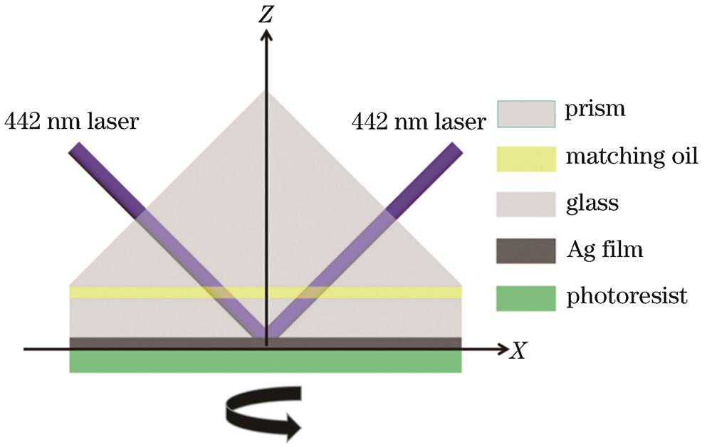
    Fig. 1. Schematic of high-order waveguide mode interference lithography by continuously rotating sample
    Simulated optical field distribution of TE5 waveguide mode interference for 1200-nm thickness photoresist
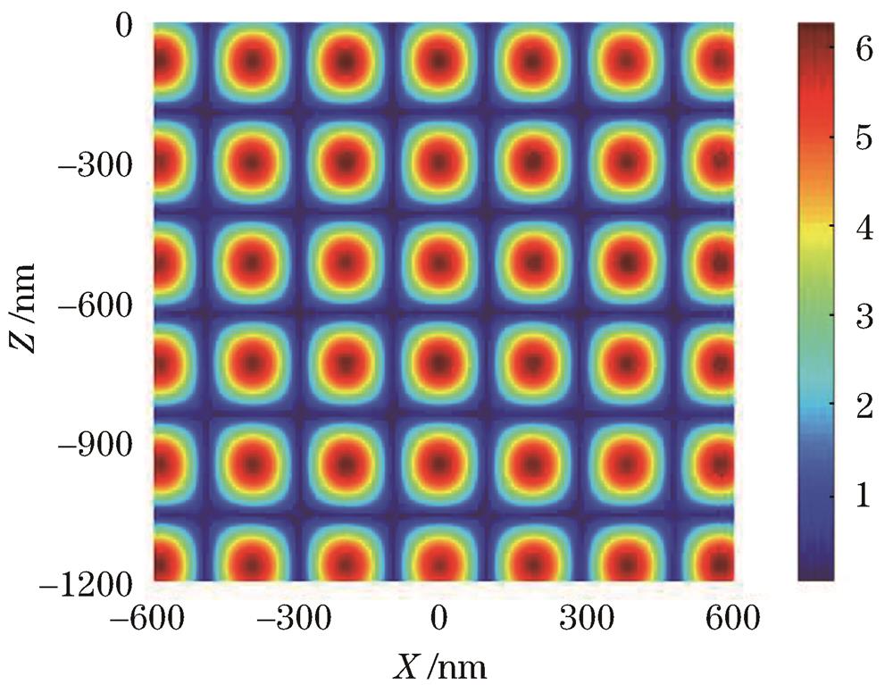
    Fig. 2. Simulated optical field distribution of TE5 waveguide mode interference for 1200-nm thickness photoresist
    Optical field distribution in photoresist after continuously rotating and exposing sample by interference field of TE5. (a) Three-dimensional optical field distribution; (b) optical field distribution corresponding to Fig. 3(a) cutting from plane Y= 0 nm; (c) optical filed distribution of X-Y plane with Z= -300 nm in Fig. 3(a); (d) optical filed distribution of X-Z plane with Y= 0 nm in Fig. 3(a); (e) optical field intensity distribution along X-axis from -600 to 600 nm with Y= 0 nm and Z=-300 nm in Fig. 3(c); (f) optical field intensity distribution along Z-axis from -1200 to 0 nm with X= 0 nm and Y= 0 nm in Fig. 3(d)
    Fig. 3. Optical field distribution in photoresist after continuously rotating and exposing sample by interference field of TE5. (a) Three-dimensional optical field distribution; (b) optical field distribution corresponding to Fig. 3(a) cutting from plane Y= 0 nm; (c) optical filed distribution of X-Y plane with Z= -300 nm in Fig. 3(a); (d) optical filed distribution of X-Z plane with Y= 0 nm in Fig. 3(a); (e) optical field intensity distribution along X-axis from -600 to 600 nm with Y= 0 nm and Z=-300 nm in Fig. 3(c); (f) optical field intensity distribution along Z-axis from -1200 to 0 nm with X= 0 nm and Y= 0 nm in Fig. 3(d)
    Optical field distribution in photoresist after continuously rotating and exposing sample by interference field of TM51. (a) Three-dimensional optical field distribution; (b) optical field distribution corresponding to Fig. 4(a) cutting from plane Y= 0 nm; (c) optical filed distribution of X-Y plane with Z= 0 nm in Fig. 4 (a); (d) optical filed distribution of X-Z plane with Y= 0 nm in Fig. 4 (a); (e) optical field intensity distribution along X-axis from -1000 to 1000 nm with Y= 0 nm and Z= 0 nm in Fig. 4 (c); (f) optical field intensity distribution along Z-axis from -2000 to 0 nm with X= 0 nm and Y= 0 nm in Fig. 4(d)
    Fig. 4. Optical field distribution in photoresist after continuously rotating and exposing sample by interference field of TM51. (a) Three-dimensional optical field distribution; (b) optical field distribution corresponding to Fig. 4(a) cutting from plane Y= 0 nm; (c) optical filed distribution of X-Y plane with Z= 0 nm in Fig. 4 (a); (d) optical filed distribution of X-Z plane with Y= 0 nm in Fig. 4 (a); (e) optical field intensity distribution along X-axis from -1000 to 1000 nm with Y= 0 nm and Z= 0 nm in Fig. 4 (c); (f) optical field intensity distribution along Z-axis from -2000 to 0 nm with X= 0 nm and Y= 0 nm in Fig. 4(d)
    Yingwen Su, Zhenyu Chen, Yueqi Xu, Xiangxian Wang. Multi-Layer Subwavelength Circular Grating Fabricated by High-Order Waveguide Mode Interference and Continuous Sample Rotation[J]. Laser & Optoelectronics Progress, 2022, 59(11): 1122001
    Download Citation