
Zheng-Qiong Dong, Hang Zhao, Jin-Long Zhu, Ya-Ting Shi. Influence of incident illumination on optical scattering measurement of typical photoresist nanostructure [J]. Acta Physica Sinica, 2020, 69(3): 030601-1
- Acta Physica Sinica
- Vol. 69, Issue 3, 030601-1 (2020)
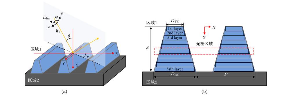
Fig. 1. (a) Geometry of the trapezoidal groove line grating; (b) layers division for inverse modeling based on RCWA.(a) 线条光栅结构的几何形貌示意图; (b) RCWA建模的分层示意图
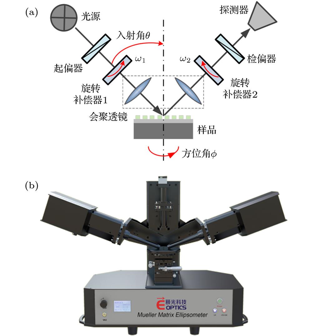
Fig. 2. Principle and instrument of the dual rotating-compensator Mueller matrix ellipsometer: (a) Principle; (b) instrument.双旋转补偿器型Mueller矩阵椭偏仪 (a)基本光路; (b)仪器
Fig. 3. (a) The SiO2 sample; (b) the PMMA sample spinning coated on the surface of the SiO2 film.
(a) SiO2薄膜样品; (b) 在SiO2表面旋涂PMMA光刻胶后的薄膜样品
Fig. 4. Extracted results of the thicknesses of SiO2 film h 1 and equivalent surface roughness r 1: (a) r 1; (b) d 1; (c) MSE.
拟合得到的20组SiO2膜厚d 1及其表面粗糙度等效膜厚r 1 (a) r 1; (b) d 1; (c) MSE
Fig. 5. Extracted results of the optical constants n 1 and k 1 of SiO2 film calculated by Cauchy model and the ones from Ref. [34]: (a) n 1; (b) k 1.
拟合得到的第1, 5, 10, 15和20组SiO2薄膜光学常数n 1和k 1的计算值, 以及文献[34]给出的折射率与消光系数 (a) n 1; (b) k 1
Fig. 6. Extracted results of the thicknesses of PMMA film d 2 and equivalent surface roughness r 2: (a) r 2; (b) d 2; (c) MSE.
拟合得到的20组PMMA膜厚d 2及其表面粗糙度等效膜厚r 2 (a) r 2; (b) d 2; (c) MSE
Fig. 7. Extracted results of the optical constants n 2 and k 2 of PMMA film calculated by Cauchy model: (a) n 2; (b) k 2拟合得到的第1, 5, 10, 15和20组PMMA薄膜光学常数n 2和k 2的计算值 (a) n 2; (b) k 2
Fig. 8. Geometry of the simulated PMMA grating samplePMMA光刻胶仿真光栅的结构示意图
Fig. 9. Fitting results of the calculated and the “ellipsometer-measured” Mueller matrix elements at the incidence and azimuthal angles fixed at θ = 65° and φ = 0°.
在入射角θ = 65°、方位角φ = 0°的入射条件下, PMMA光刻胶仿真光栅的模型计算Mueller矩阵光谱与“测量”光谱之间的拟合曲线
|
Table 1. Comparison of these three true dimensions and the extracted results of the simulated PMMA grating.

Set citation alerts for the article
Please enter your email address
© Copyright 2018-2021 | Chinese Laser Press. All Rights Reserved 沪ICP备15018463号-20