• Photonics Research
  • Vol. 8, Issue 2, 103 (2020)
Houkai Chen1、†, Yuquan Zhang1、†, Yanmeng Dai1、†, Changjun Min1、3、*, Siwei Zhu2, and Xiaocong Yuan1、4、*
Author Affiliations
  • 1Nanophotonics Research Center, Shenzhen Key Laboratory of Micro-Scale Optical Information Technology, Shenzhen University, Shenzhen 518060, China
  • 2Tianjin Union Medical Center, Tianjin 300121, China
  • 3e-mail: cjmin@szu.edu.cn
  • 4e-mail: xcyuan@szu.edu.cn
  • show less
    DOI: 10.1364/PRJ.8.000103 Cite this Article Set citation alerts
    Houkai Chen, Yuquan Zhang, Yanmeng Dai, Changjun Min, Siwei Zhu, Xiaocong Yuan. Facilitated tip-enhanced Raman scattering by focused gap-plasmon hybridization[J]. Photonics Research, 2020, 8(2): 103 Copy Citation Text show less
    (a) Schematic of the TERS system. 4-Q PD, 4-quadrant photodiode; WPV, zero-order vortex half-wave retarder plate; BS, beam splitter. (b) Schematic of the virtual SP probe-excited TERS on a gold film. RP beam indicates the radially polarized incident beam.
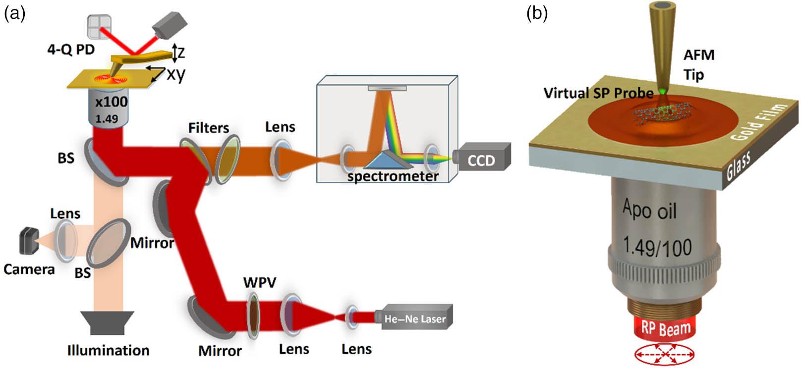
    Fig. 1. (a) Schematic of the TERS system. 4-Q PD, 4-quadrant photodiode; WPV, zero-order vortex half-wave retarder plate; BS, beam splitter. (b) Schematic of the virtual SP probe-excited TERS on a gold film. RP beam indicates the radially polarized incident beam.
    Numerical calculation of the electric field normalized to the traditional tightly focused electric field. (a) Schematic of the tip on glass. (b) Calculated electric field |E|2 distribution of the gold-coated tip apex on glass substrate excited by a tightly focused radially polarized 632.8 nm laser. (c) Profiles of the electric field |E|2 along the line through the center plane of the gap volume. (d) Schematic of the tip on gold film. (e) Calculated electric field |E|2 distribution of the gold-coated tip apex on gold film. (f) Profiles of the electric field |E|2 with different gold coating thicknesses. The yellow dashed lines denote the surface of the substrate and the tip apex. Axes units in (b) and (e): nm.
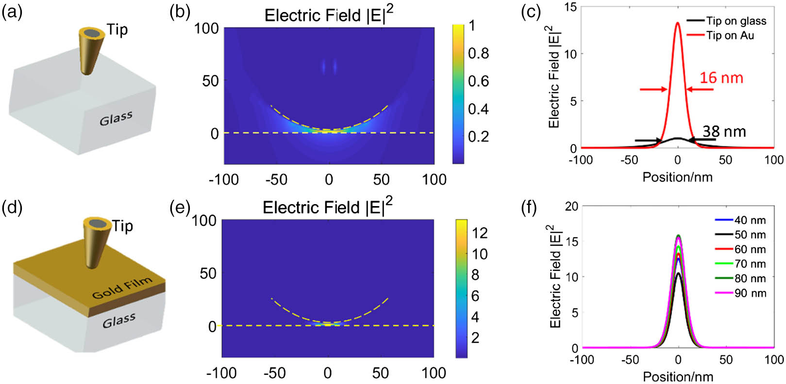
    Fig. 2. Numerical calculation of the electric field normalized to the traditional tightly focused electric field. (a) Schematic of the tip on glass. (b) Calculated electric field |E|2 distribution of the gold-coated tip apex on glass substrate excited by a tightly focused radially polarized 632.8 nm laser. (c) Profiles of the electric field |E|2 along the line through the center plane of the gap volume. (d) Schematic of the tip on gold film. (e) Calculated electric field |E|2 distribution of the gold-coated tip apex on gold film. (f) Profiles of the electric field |E|2 with different gold coating thicknesses. The yellow dashed lines denote the surface of the substrate and the tip apex. Axes units in (b) and (e): nm.
    (a) SEM image of the gold-coated AFM tip with a thickness of 60 nm; (b) Raman spectra of self-assembled 4-MBA layer measured when the tip was in the engaged mode (red curve) and withdrawn (black curve) mode; (c) spectral measurements on glass substrate with (red curve) and without (black curve) the metallic tip; incident laser, 632.8 nm, ∼1.8 mW; integration time, 1 s.
    Fig. 3. (a) SEM image of the gold-coated AFM tip with a thickness of 60 nm; (b) Raman spectra of self-assembled 4-MBA layer measured when the tip was in the engaged mode (red curve) and withdrawn (black curve) mode; (c) spectral measurements on glass substrate with (red curve) and without (black curve) the metallic tip; incident laser, 632.8 nm, 1.8  mW; integration time, 1 s.
    (a) AFM image of SWCNT bundles deposited on the gold film; (b) height profile along the white dashed line in (a); (c) TERS signal along the dashed line in (a) at the Raman peak of the G-band at 1590 cm−1; (d) Raman spectra at positions A and B denoted in (a); laser power, ∼1.8 mW; integration time, 1 s.
    Fig. 4. (a) AFM image of SWCNT bundles deposited on the gold film; (b) height profile along the white dashed line in (a); (c) TERS signal along the dashed line in (a) at the Raman peak of the G-band at 1590  cm1; (d) Raman spectra at positions A and B denoted in (a); laser power, 1.8  mW; integration time, 1 s.
    (a) AFM image of SWCNT bundles deposited on the gold film; (b) TERS imaging at the Raman peak of 1590 cm−1 according to the white dashed region in (a); laser power, ∼1.8 mW; integration time, 1 s.
    Fig. 5. (a) AFM image of SWCNT bundles deposited on the gold film; (b) TERS imaging at the Raman peak of 1590  cm1 according to the white dashed region in (a); laser power, 1.8  mW; integration time, 1 s.
    Houkai Chen, Yuquan Zhang, Yanmeng Dai, Changjun Min, Siwei Zhu, Xiaocong Yuan. Facilitated tip-enhanced Raman scattering by focused gap-plasmon hybridization[J]. Photonics Research, 2020, 8(2): 103
    Download Citation