Tip-enhanced Raman scattering (TERS) spectroscopy is a nondestructive and label-free molecular detection approach that provides high sensitivity and nanoscale spatial resolution. Therefore, it has been used in a wide array of applications. We demonstrate a gap-plasmon hybridization facilitated by a bottom-illuminated TERS configuration. The gap-plasmon hybridization effect is first performed with the finite-difference time-domain method to optimize the parameters, and experiments are then conducted to calibrate the performance. The results demonstrate an enhancement factor of 1157 and a spatial resolution of 13.5 nm. The proposed configuration shows great potential in related surface imaging applications in various fields of research.
1. INTRODUCTION
The tip-enhanced Raman scattering (TERS) technique, with the benefits of high spatial resolution and high sensitivity, is a powerful imaging tool for optical characterizations of nanomaterials and surface catalysts [1–12]. These advantages are derived from the localized electromagnetic field excited on the metallic tip of a scanning probe microscope. This localized field results in nanoscale spatial resolution, as well as greatly enhanced intensity. Therefore, the Raman spectra of samples confined in the vicinity of the tip apex experience a greatly enhanced detection sensitivity on the single-molecule level. Scanning tunneling microscopy (STM) has widely been used in TERS imaging and has achieved an angstrom-scale spatial resolution for single-molecule chemical imaging under special experimental conditions [12–14]. Atomic force microscopy (AFM)-based TERS systems, which can easily work in atmospheric and liquid environments, have great superiority in a wide range of research fields, such as biology studies in a native environment. So far, a subnanometer resolution has been achieved on an AFM-TERS platform, [15] and many interesting results have been reported [16–22].
Related research demonstrated that a metallic substrate exerts prominent effects on the performance of the TERS technique [23–25], where the nanogap mode offers a higher enhancement in a smaller resonance volume. The gap-plasmon hybridization provides a high sensitivity and spatial resolution owing to the coupling between the substrate and metallic tip apex. However, this case is mainly employed in side- and top-illumination configurations, because the metallic substrate blocks the exciting source in the bottom-illumination configuration. Some improvements have been proposed, such as employing a plasmonic lens to focus the surface plasmon (SP) wave on the metallic substrate surface to form a gap plasmon with higher enhancement [26]. However, the structured substrate was not suitable for scanning imaging applications.
Here, we use a virtual SP probe that is excited on a thin metallic film with a highly focused laser beam in a bottom-illumination configuration, where the field intensity enhancement is almost 1 order of magnitude compared with the exciting source [27,28]. The focused SP provides a much purer longitudinal electric field, which excites a more localized hot spot to dominate the enhancement in this configuration. Compared with the conventionally focused laser beam, the stimulated gap-plasmon hybridization between the virtual SP probe and AFM tip leads to greater enhancement and higher resolution. The simulated and experimental results both demonstrated these virtues. Furthermore, as the focused plasmonic probe is able to be dynamically controlled on a smooth surface, extensive application prospects are possible in molecular detection and scanning imaging applications.
Sign up for Photonics Research TOC. Get the latest issue of Photonics Research delivered right to you!Sign up now
2. METHODS
A. Experimental Configuration
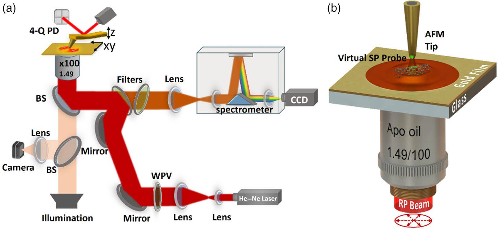
The experimental system is illustrated in Fig. 1(a), which was integrated with three functional modules: an inverted optical microscope (Ti-u, Nikon Inc.) to modulate the light source; a bioscope catalyst AFM platform (Bruker Inc.), mounted onto the microscope to perform sample morphology imaging; and a confocal raster spectrometer (inVia, Renishaw Inc.) to obtain the spectrum. The 632.8-nm laser beam was first expanded to fit the aperture of the objective, and then its polarization state was converted from linear polarization into radial polarization by a zero-order half-wave vortex retarder plate (WVP10L-633, Thorlabs Inc.), satisfying the polarization condition of SP excitation at a ring-shaped position. The surface plasmonic field was excited on the 45-nm gold film coated on a glass substrate by a tightly focused laser through an oil-immersion objective with a high NA of 1.49 (Apo, , Nikon Inc.), as shown in Fig. 1(b). Such a high NA can meet with the demands of the incident angle for SP. The plasmons were then focused into the center to form a virtual SP probe with a higher intensity [27].
Figure 1.(a) Schematic of the TERS system. 4-Q PD, 4-quadrant photodiode; WPV, zero-order vortex half-wave retarder plate; BS, beam splitter. (b) Schematic of the virtual SP probe-excited TERS on a gold film. RP beam indicates the radially polarized incident beam.
As the enhancement factor (EF) in a gap-mode TERS system is highly related to the longitudinal field intensity, such a configuration could provide highly efficient gap-mode Raman enhancement in the bottom-illumination TERS setup. Subsequently, a hot spot could be excited when the tip was near the gold film to obtain an enhanced Raman spectrum of the sample. The backscattered TERS signals could be collected by the objective, and the Rayleigh scattering light was blocked by edge-pass filters. After diffraction through a 1800-lines/mm grating in the spectrometer, the spectral information was recorded by a CCD camera for further analysis. Although the Raman scattering signal was collected through the gold film, which could block the scattering signals, the surface-plasmon-coupled emission (SPCE) phenomenon could ensure the highly efficient detection of the TERS signals [29]. Samples on the substrate were actuated by a piezoelectric mapping stage inserted in the mechanical stage, and its distribution could be first mapped by the AFM system to help to select the detection area. The actuator of the AFM was aligned with the spectrometer to get a synchronous measurement of the Raman scattering signal and tip positioning.
B. Tip Fabrication
As has been demonstrated in previous work, the metal coating of the probe exerts a large influence on the intensity of the excited hot spots and the Raman signal [23]. Here, to achieve a higher EF, the AFM tip was first modified with a thin gold cladding. The tips were coated using a thermal evaporation system (VZZ-300, KYKY Technology Inc.) at , where the tips were located on an inverted horizontal substrate. The deposition rate was set as 0.2–0.3 Å/s by regulating the current, which was aimed at obtaining a relatively smooth cladding with low roughness. The tip with a 60-nm-thick gold film was used in the following experiments. The coated tips were stored in a vacuum tank for use. In the experiments, the AFM worked in the contact mode to scan the sample between the metallic tip and thin gold film.
C. Sample Preparation
To characterize the detection sensitivity of the TERS system, a self-assembled monolayer of 4-mercaptobenzoic acid (4-MBA, Sigma-Aldrich, U.S.) was fabricated as a uniform molecular probe. Briefly, the gold coating substrate was first immersed in a mol/L 4-MBA methanol solution for 10 min to form the self-assembled monolayer on the gold film. Then, the substrate was flushed with ethanol solution to rinse off the excess molecules, to ensure the thickness uniformity of the molecular layer.
Single-walled carbon nanotubes (SWCNTs), as well-studied one-dimensional materials for Raman imaging, were employed to characterize the spatial resolution of our TERS system. SWCNTs were dissolved in deionized water with an appropriate concentration, and then were dropped onto the gold film surface.
3. RESULTS AND DISCUSSION
A. Numerical Simulations
The gold cladding was able to exert a great influence on the excited Raman signals [30]. As a consequence, an optimized parameter was needed to achieve a huge enhancement as well as a high resolution. The numerical simulations were first performed based on the finite-difference time-domain (FDTD) method to research the interaction between the virtual SP probe and the metalized AFM tip. In accordance with the experiments, the silicon AFM probe was set as a three-dimensional (3D) cone with a half-cone angle of 10° and an apex radius of 20 nm. The gap distance between the tip apex and the substrate surface was 2 nm. The excitation source was a 632.8 nm radially polarized beam illuminating from the bottom, which was an ideal choice for its high performance on the TERS response of the gold-coated tip. The material parameters were fitted using the Johnson–Christy mode. The perfectly matched layer (PML) boundary condition was used for all simulations. To guarantee numerical accuracy, a 0.5-nm mesh was employed. To clearly show the electric field enhancement, all the calculated results were normalized according to the enhanced electric field with the 60-nm thin gold cladding tip on a glass substrate.
To show the advantages of the gap-plasmon hybridization between the metallic surface and the metal-clad tip, a generic gold cladding thickness of 60 nm was first selected and calculated for analysis in Fig. 2(a). The calculation result on a bare glass substrate is shown in Fig. 2(b), where a strong hot spot was excited on the tip apex. The electromagnetic field was greatly confined on the apex and was quickly attenuated when moving away from the tip apex. Consequently, the scattering enhancement could only be achieved in the area very close to the tip apex. The electric field along the center line (the black one) in Fig. 2(c) clearly demonstrates this fact. Then the metal substrate was induced for the huge enhancement of electromagnetic field in the gap mode. As has been demonstrated, the focused SP virtual probe could be formed on a 45-nm gold-coated glass substrate, which naturally showed an enhanced intensity compared with the laser focus field. Owing to the gap-plasmon hybridization effects, when the tip was near the SP probe, an additional enhancement was achieved, which resulted from the nanogap mode mechanism between the metallic cladding on the tip and the gold film, as shown in Fig. 2(d), with the other parameters kept the same as in Fig. 2(a). The calculated intensity of the electric field result is shown in Fig. 2(e), which was more than 1 order of magnitude higher than that without the gold film. Furthermore, the electric field was more confined in a much smaller volume under the tip apex. The calculated result explicitly demonstrated the impact of the plasmonic hybridization in TERS for better performance.
The spatial resolution is another important factor in the TERS imaging system, which is closely related to the size of the hot spot. According to the electric field plotted in Fig. 2(c), the full width at half-maximum (FWHM) of the electric field was approximately 38 nm, which was much smaller than a conventional focused light spot and the tip apex. As the coated thin gold film on the substrate induced gap-plasmon hybridization effects, the FWHM of the facilitated hot spot was further suppressed to approximately 16 nm, which was more than twofold compressed compared with the case of a tip on a glass substrate. Further, considering that the Raman signal is nearly proportional to the fourth power of the electric field amplitude [31], the spatial resolution of the Raman signal will be approximately 11 nm. If other factors are considered, the resolution will be further improved [32,33]. Therefore, the nanosized hot spot provides the possibility for an ultrahigh spatial resolution.
The gold coating thickness of the tip apex is known to exert an influence on the coupling between the electromagnetic field and the metallic tip [23]. We further calculated the electric field distribution in the gap with different coating thicknesses of 40, 50, 60, 70, 80, and 90 nm. The results in Fig. 2(f) show that the enhanced electric field magnitude was of the same order for all cases, where the 80-nm coating had the highest enhancement, while the 50-nm coating had the lowest. However, the thicker coating could reduce the spatial resolution capability because it meant a larger size of the tip apex to decrease the locality of the electric field. According to the simulations, the 50-nm coating had the highest spatial resolution among these tips, which was closely followed by the tips with a coating thickness of 40 and 60 nm. Consequently, the balance between the electric field enhancement and spatial resolution is still worthy of consideration for TERS research. The simulations demonstrated that the negative effects of the coating thickness on the spatial resolution were relatively slight. Here, after comprehensive consideration, a 60-nm coating was employed in the following experiments.
B. Experiments
The detection sensitivity of the TERS system is typically characterized by the EF, and for the present configuration, it can be defined by the following equation [34]: where and are the Raman intensities measured with and without the tip, is the area of the focused virtual SP spot in this work, and is the area of the excited hybridized localized surface plasmon (LSP) at the tip apex, given that the molecular density is constant on the substrate surface.
To quantify the EF of the TERS system, a 4-MBA self-assembled monolayer on the gold film was employed as a uniform substrate. Experimentally, a metallic tip with 60-nm-thick gold cladding was used, and its scanning electron microscopy (SEM, Phenom ProX, Finland) image is shown in Fig. 3(a). The Raman signals were measured twice at the same position with the tip engaged to the substrate and lifted approximately 1 μm from the substrate surface, respectively. The baseline of each Raman spectrum was subtracted using Renishaw’s WiRE function module (Version 4.3). The results in Fig. 3(b) explicitly show the impact of the gold tip on the enhancement of the scattering signal. In order to calculate the EF, the parameters of and were obtained from the FDTD simulations, and the Raman intensities and were directly acquired from the engage data and withdraw data at in Fig. 3(b). Finally, the EF was estimated to be approximately 1157.
Figure 2.Numerical calculation of the electric field normalized to the traditional tightly focused electric field. (a) Schematic of the tip on glass. (b) Calculated electric field distribution of the gold-coated tip apex on glass substrate excited by a tightly focused radially polarized 632.8 nm laser. (c) Profiles of the electric field along the line through the center plane of the gap volume. (d) Schematic of the tip on gold film. (e) Calculated electric field distribution of the gold-coated tip apex on gold film. (f) Profiles of the electric field with different gold coating thicknesses. The yellow dashed lines denote the surface of the substrate and the tip apex. Axes units in (b) and (e): nm.
Figure 3.(a) SEM image of the gold-coated AFM tip with a thickness of 60 nm; (b) Raman spectra of self-assembled 4-MBA layer measured when the tip was in the engaged mode (red curve) and withdrawn (black curve) mode; (c) spectral measurements on glass substrate with (red curve) and without (black curve) the metallic tip; incident laser, 632.8 nm, ; integration time, 1 s.
From the definition equation, we can see that the EF is only an estimate. Different from the estimated EF, the contrast, which is defined by depending on the experimental data, is more instinctive and is widely used to gauge the performance of the TERS tip [22]. In our system, the tip could provide a -fold increase in TERS contrast. For comparison, the experiments of TERS on a glass substrate were conducted; the results are shown in Fig. 3(c). Although the enhancement of the metallic tip was intuitive, the signal-to-noise ratio (SNR) of the TERS spectrum (the red curve) was lower than the signal with the gap-plasmon hybridization. This result was consistent with the aforementioned simulations.
The TERS imaging experiment on SWCNTs was implemented to demonstrate its spatial resolution and its advantageous performance, as shown in Fig. 4. The 3D morphology profiles of the sample were first confirmed using AFM in the contact mode, as shown in Fig. 4(a). The topographic profile of the SWCNT sample along the white dashed line in Fig. 4(a) is shown in Fig. 4(b). Taking the fitting data (height 7.3 nm, FWHM 43 nm) into consideration, the radius of the tip was estimated to be . Then, the TERS signals were measured point-by-point along the same dashed line, while keeping the AFM tip working in the contact mode. The Raman signal of the G-band of the SWCNTs () was plotted as the black curve shown in Fig. 4(c). The background noise was suppressed when we fitted the curve to quantify the spatial resolution capability using the Gaussian function, as shown in Fig. 4(c). The Raman spectra at positions A (at the sample) and B with a distance of around 58 nm as denoted in Fig. 4(a) were plotted in Fig. 4(d). The signal of the D-band was also clearly observed.
The resolution of the TERS system should be no less than 13.5 nm according to the FWHM of the red fitted curve. The results showed that TERS was able to achieve a higher spatial resolution than AFM. This was in good agreement with the aforementioned simulation results and can also be easily understood. The AFM image showed the convolution of the tip apex and the sample, and its spatial resolution depended on the size of the tip. It is widely accepted that the spatial resolution of TERS depends largely on the LSP of the tip apex, which is closely related to the tip apex size and the tip–substrate distance, and is usually much smaller than the tip apex.
To further validate the imaging capability of the hybridized TERS technique, two-dimensional (2D) scanning imaging of the SWCNTs was conducted in the contact mode. Figure 5(a) shows the morphology of the SWCNT bundles, and the Raman peak of the G-band is plotted in Fig. 5(b), which clearly showed the distribution of the SWCNTs. The data were interpolated using MATLAB function imresize( ). These results validated the feasibility of hybridized TERS as an effective approach in chemical imaging.
Figure 4.(a) AFM image of SWCNT bundles deposited on the gold film; (b) height profile along the white dashed line in (a); (c) TERS signal along the dashed line in (a) at the Raman peak of the G-band at ; (d) Raman spectra at positions A and B denoted in (a); laser power, ; integration time, 1 s.
Figure 5.(a) AFM image of SWCNT bundles deposited on the gold film; (b) TERS imaging at the Raman peak of according to the white dashed region in (a); laser power, ; integration time, 1 s.
It is worth mentioning that the electrical enhancement in the gap-plasmon mode was only 1 order of magnitude higher than that in the case without a metal film on the substrate, which was not as high as expected. This can be easily understood. In the traditional bottom-illumination configuration, the substrate is usually transparent, and all incident light waves at various incident angles can interact with the metalized tip and contribute to the electric field enhancement to various extents. However, in the presented SP-stimulated TERS configuration, only a few light beams at certain incident angles could satisfy the SP resonance excitation condition at the gold/air interface to generate the virtual SP probe, and most of the incident light is reflected from the substrate. This decreased the coupling efficiency of the illumination system, decreasing the enhancement of the electric field in the gap. This shortcoming can be lessened if an annular-shaped radially polarized incident beam is used and its incident angle matches the SP resonance angle [35,36]. Furthermore, the enhancement and spatial resolution of TERS imaging are greatly dependent on the tip apex, for example, coating thickness and tilt angles. As a consequence, the performance could be further optimized by improving the tips and incident light for both higher spatial resolution and detection sensitivity.
4. CONCLUSIONS
In summary, we proposed a facilitated bottom-illuminated TERS configuration in virtue of the gap-plasmon hybridization effects. A focused plasmonic virtual probe is excited on a smooth film surface by a tightly focused, radially polarized beam. Owing to the plasmonic hybridization effects with a metallic tip in the gap region, a further confined hot spot with a higher intensity and smaller size is generated, compared with the traditional forms. These performances are verified through simulations using the 3D FDTD method. Furthermore, an optimized parameter was selected to experimentally validate the TERS mechanism. The results illustrate the advancements and practicalities of the configuration, and this technique should have great potential in related surface imaging applications in various research fields.
[15] X. M. Lin, T. Deckertgaudig, P. Singh, M. Siegmann, S. Kupfer, Z. Zhang, S. Gräfe, V. Deckert. Direct base-to-base transitions in ssDNA revealed by tip-enhanced Raman scattering(2016).