• Photonics Research
  • Vol. 12, Issue 3, 522 (2024)
Zijian Liu1、†, Yuying Xi1、†, Wenbo Zeng1, Ting Ji1、3、*, Wenyan Wang1, Sitong Guo1, Linlin Shi1, Rong Wen1, Yanxia Cui1、2、4、*, and Guohui Li1、2、5、*
Author Affiliations
  • 1College of Physics, College of Electronic Information and Optical Engineering, Key Laboratory of Advanced Transducers and Intelligent Control System of Ministry of Education, Taiyuan University of Technology, Taiyuan 030024, China
  • 2Shanxi-Zheda Institute of Advanced Materials and Chemical Engineering, Taiyuan 030032, China
  • 3e-mail: jiting@tyut.edu.cn
  • 4e-mail: yanxiacui@tyut.edu.cn
  • 5e-mail: liguohui@tyut.edu.cn
  • show less
    DOI: 10.1364/PRJ.502892 Cite this Article Set citation alerts
    Zijian Liu, Yuying Xi, Wenbo Zeng, Ting Ji, Wenyan Wang, Sitong Guo, Linlin Shi, Rong Wen, Yanxia Cui, Guohui Li. Lead-free perovskite Cs2AgBiBr6 photodetector detecting NIR light driven by titanium nitride plasmonic hot holes[J]. Photonics Research, 2024, 12(3): 522 Copy Citation Text show less
    Schematic flow chart illustrating the fabrication process of the plasmonic perovskite Cs2AgBiBr6 PD incorporated with TiN NPs and Al2O3 ultrathin layer. (a) Preparing a hydrophilic glass substrate; (b) forming a single layer of highly ordered closely packed PS nanospheres on glass substrate obtained by self-assembly method; (c) obtaining sparsely distributed PS nanosphere array by the RIE method; (d) depositing a TiN layer with a thickness of 40 nm by the RF magnetron sputtering method; (e) obtaining TiN NP array on the glass substrate after removing PS spheres; (f) depositing an ultrathin Al2O3 layer on the above formed TiN NPs by ALD; (g) spin coating the Cs2AgBiBr6 thin film on the Al2O3 interfacial layer; and (h) sputtering TiN electrodes with a thickness of 80 nm on Cs2AgBiBr6 using a copper mesh as the mask. In (h), the light is incident on the PD from the glass side. (i) 3D AFM image of the obtained TiN NPs.
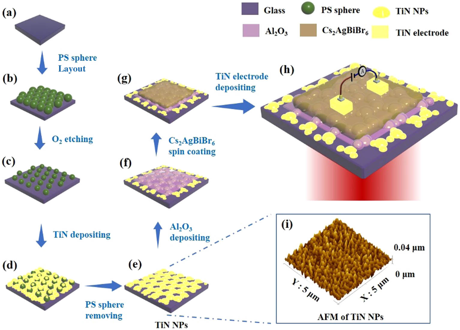
    Fig. 1. Schematic flow chart illustrating the fabrication process of the plasmonic perovskite Cs2AgBiBr6 PD incorporated with TiN NPs and Al2O3 ultrathin layer. (a) Preparing a hydrophilic glass substrate; (b) forming a single layer of highly ordered closely packed PS nanospheres on glass substrate obtained by self-assembly method; (c) obtaining sparsely distributed PS nanosphere array by the RIE method; (d) depositing a TiN layer with a thickness of 40 nm by the RF magnetron sputtering method; (e) obtaining TiN NP array on the glass substrate after removing PS spheres; (f) depositing an ultrathin Al2O3 layer on the above formed TiN NPs by ALD; (g) spin coating the Cs2AgBiBr6 thin film on the Al2O3 interfacial layer; and (h) sputtering TiN electrodes with a thickness of 80 nm on Cs2AgBiBr6 using a copper mesh as the mask. In (h), the light is incident on the PD from the glass side. (i) 3D AFM image of the obtained TiN NPs.
    (a) SEM image; (b) XRD pattern and (c) absorption spectrum of the Cs2AgBiBr6 film; (d) absorption versus photo energy of the Cs2AgBiBr6 film for deriving the bandgap; (e) steady-state PL spectra and (f) measured absorption spectra of the prepared films of Cs2AgBiBr6 and Cs2AgBiBr6/Al2O3/TiN NPs, respectively.
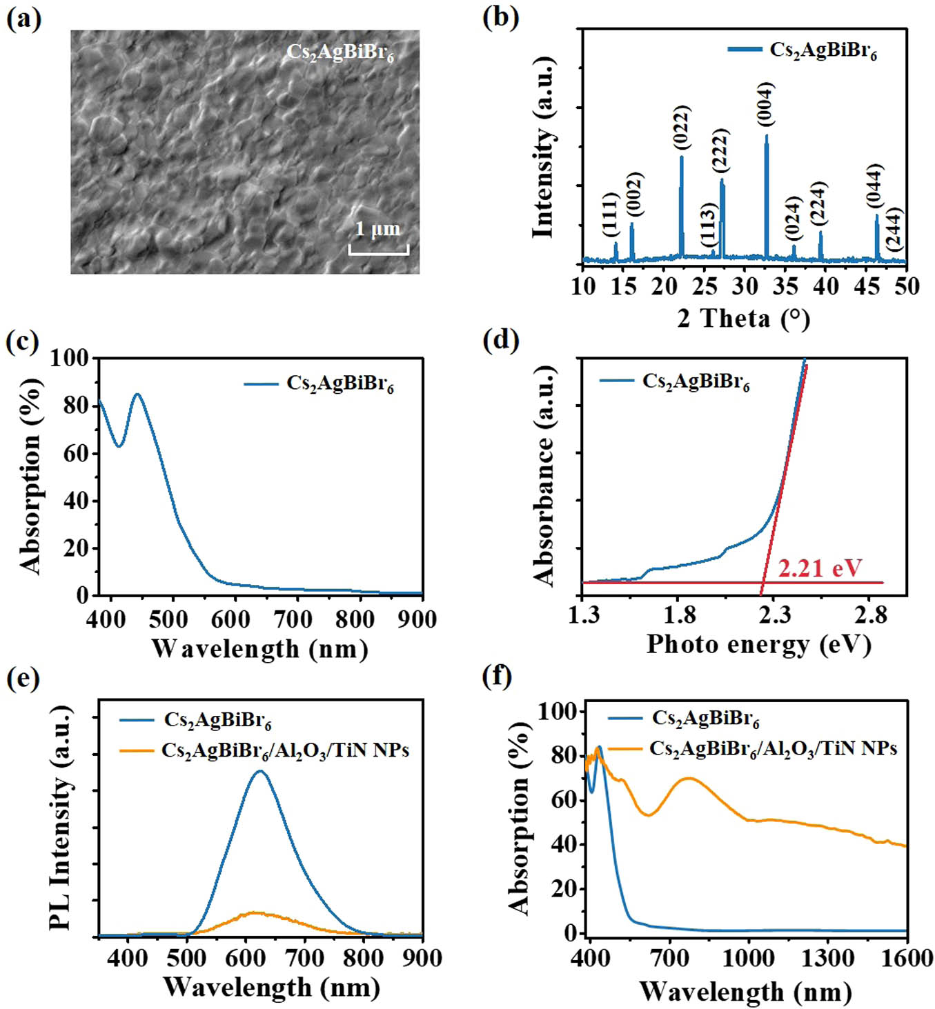
    Fig. 2. (a) SEM image; (b) XRD pattern and (c) absorption spectrum of the Cs2AgBiBr6 film; (d) absorption versus photo energy of the Cs2AgBiBr6 film for deriving the bandgap; (e) steady-state PL spectra and (f) measured absorption spectra of the prepared films of Cs2AgBiBr6 and Cs2AgBiBr6/Al2O3/TiN NPs, respectively.
    (a) I–V curves of Cs2AgBiBr6, Cs2AgBiBr6/TiN NPs, and Cs2AgBiBr6/Al2O3/TiN NP devices measured in the dark. (b) and (c) I–V curves of the Cs2AgBiBr6, Cs2AgBiBr6/TiN NP, and Cs2AgBiBr6/Al2O3/TiN NP devices under 505 and 850 nm light illuminations. Insets, transient photocurrent responses of the Cs2AgBiBr6 and Cs2AgBiBr6/Al2O3/TiN NP devices at 505 and 850 nm, respectively; (d) transient photocurrent curves of the Cs2AgBiBr6 device and Cs2AgBiBr6/Al2O3/TiN NP device at 505 and 850 nm; (e) LDR characterization of the Cs2AgBiBr6/Al2O3/TiN NP device measured under 505 and 850 nm illuminations at 1 V; (f)–(h) EQE, R, and D* of the Cs2AgBiBr6 and Cs2AgBiBr6/Al2O3/TiN NP devices at different wavelengths; (i) measured noise currents of the Cs2AgBiBr6 and Cs2AgBiBr6/Al2O3/TiN NP devices at various frequencies at 1 V bias. The calculated shot noise and thermal noise limits are also included for reference.
    Fig. 3. (a) IV curves of Cs2AgBiBr6, Cs2AgBiBr6/TiN NPs, and Cs2AgBiBr6/Al2O3/TiN NP devices measured in the dark. (b) and (c) IV curves of the Cs2AgBiBr6, Cs2AgBiBr6/TiN NP, and Cs2AgBiBr6/Al2O3/TiN NP devices under 505 and 850 nm light illuminations. Insets, transient photocurrent responses of the Cs2AgBiBr6 and Cs2AgBiBr6/Al2O3/TiN NP devices at 505 and 850 nm, respectively; (d) transient photocurrent curves of the Cs2AgBiBr6 device and Cs2AgBiBr6/Al2O3/TiN NP device at 505 and 850 nm; (e) LDR characterization of the Cs2AgBiBr6/Al2O3/TiN NP device measured under 505 and 850 nm illuminations at 1 V; (f)–(h) EQE, R, and D* of the Cs2AgBiBr6 and Cs2AgBiBr6/Al2O3/TiN NP devices at different wavelengths; (i) measured noise currents of the Cs2AgBiBr6 and Cs2AgBiBr6/Al2O3/TiN NP devices at various frequencies at 1 V bias. The calculated shot noise and thermal noise limits are also included for reference.
    (a) EQE and absorption enhancement factors at different wavelengths; (b) simulated absorption spectra of the Cs2AgBiBr6 and Cs2AgBiBr6/TiN NP structures; (c) electric field distributions in the x−y plane at the simulated absorption peak of 735 nm for the Cs2AgBiBr6/TiN NP structure; (d) contact potential map of the Al2O3 modified TiN NPs taken by the KPFM technique (φ and W are the average contact potential and work function of the Al2O3 modified TiN NPs, respectively); (e) energy band diagram of the Cs2AgBiBr6/Al2O3/TiN NP device (WTiN NPs=4.92 eV, Ec=−3.6 eV, Ev=−5.7 eV, ϕb=0.78 eV); (f) working mechanism of the Cs2AgBiBr6/Al2O3/TiN NP device, illustrating hot hole excitation and transfer driven by plasmonic resonances.
    Fig. 4. (a) EQE and absorption enhancement factors at different wavelengths; (b) simulated absorption spectra of the Cs2AgBiBr6 and Cs2AgBiBr6/TiN NP structures; (c) electric field distributions in the xy plane at the simulated absorption peak of 735 nm for the Cs2AgBiBr6/TiN NP structure; (d) contact potential map of the Al2O3 modified TiN NPs taken by the KPFM technique (φ and W are the average contact potential and work function of the Al2O3 modified TiN NPs, respectively); (e) energy band diagram of the Cs2AgBiBr6/Al2O3/TiN NP device (WTiNNPs=4.92  eV, Ec=3.6  eV, Ev=5.7  eV, ϕb=0.78  eV); (f) working mechanism of the Cs2AgBiBr6/Al2O3/TiN NP device, illustrating hot hole excitation and transfer driven by plasmonic resonances.
    Atomic force microscopy (AFM) image of the (a) monolayer polystyrene (PS) spheres and (b) sparsely-distributed PS nanosphere array.
    Fig. 5. Atomic force microscopy (AFM) image of the (a) monolayer polystyrene (PS) spheres and (b) sparsely-distributed PS nanosphere array.
    SEM images of Cs2AgBiBr6 films prepared at the acceleration speed of (a) 1400 (r/min)/s, (b) 1200 (r/min)/s, (c) 1000 (r/min)/s, and (d) 800 (r/min)/s, respectively.
    Fig. 6. SEM images of Cs2AgBiBr6 films prepared at the acceleration speed of (a) 1400 (r/min)/s, (b) 1200 (r/min)/s, (c) 1000 (r/min)/s, and (d) 800 (r/min)/s, respectively.
    (a) 3D AFM and (b) KPFM images of the Cs2AgBiBr6 film (φ and W are the average contact potential and work function of the Cs2AgBiBr6, respectively).
    Fig. 7. (a) 3D AFM and (b) KPFM images of the Cs2AgBiBr6 film (φ and W are the average contact potential and work function of the Cs2AgBiBr6, respectively).
    XRD patterns of the Cs2AgBiBr6 films prepared on the (a) surface of Al2O3 modified TiN NPs and (b) directly prepared on top of TiN NPs.
    Fig. 8. XRD patterns of the Cs2AgBiBr6 films prepared on the (a) surface of Al2O3 modified TiN NPs and (b) directly prepared on top of TiN NPs.
    Transient photocurrent characteristic of the devices switched on and off multiple times at a power density of 10.20 mW/cm2: (a) the Cs2AgBiBr6 device at 505 nm, (b) the Cs2AgBiBr6/Al2O3/TiN NPs device at 505 nm, (c) the Cs2AgBiBr6/Al2O3/TiN NPs device at 850 nm.
    Fig. 9. Transient photocurrent characteristic of the devices switched on and off multiple times at a power density of 10.20  mW/cm2: (a) the Cs2AgBiBr6 device at 505 nm, (b) the Cs2AgBiBr6/Al2O3/TiN NPs device at 505 nm, (c) the Cs2AgBiBr6/Al2O3/TiN NPs device at 850 nm.
    LDR characterization of the Cs2AgBiBr6 device under 505 nm LED measured at 1 V.
    Fig. 10. LDR characterization of the Cs2AgBiBr6 device under 505 nm LED measured at 1 V.
    I−V curves of (a) Cs2AgBiBr6 and (b) Cs2AgBiBr6/Al2O3/TiN NPs devices measured in dark and under illumination (λ=1310 nm and 1550 nm).
    Fig. 11. IV curves of (a) Cs2AgBiBr6 and (b) Cs2AgBiBr6/Al2O3/TiN NPs devices measured in dark and under illumination (λ=1310  nm and 1550 nm).
    (a) Particle size distributions of the TiN NPs. (b) Structure of the Cs2AgBiBr6/TiN NPs device utilized in simulation. (c) Measured and simulated absorption spectra of the Cs2AgBiBr6/Al2O3/TiN NPs structure. (d) Electric field distributions at multiple x−z planes at the simulated absorption peak of 735 nm. (e), (f) Electric field distributions in the x−y plane at the simulated absorption peaks of (e) 555 nm and (f) 1145 nm.
    Fig. 12. (a) Particle size distributions of the TiN NPs. (b) Structure of the Cs2AgBiBr6/TiN NPs device utilized in simulation. (c) Measured and simulated absorption spectra of the Cs2AgBiBr6/Al2O3/TiN NPs structure. (d) Electric field distributions at multiple xz planes at the simulated absorption peak of 735 nm. (e), (f) Electric field distributions in the xy plane at the simulated absorption peaks of (e) 555 nm and (f) 1145 nm.
    Contact potential map of the reference highly oriented pyrolytic graphite (HOPG) sample taken by the KPFM technique (φ and W are the average contact potential and work function of the HOPG, respectively).
    Fig. 13. Contact potential map of the reference highly oriented pyrolytic graphite (HOPG) sample taken by the KPFM technique (φ and W are the average contact potential and work function of the HOPG, respectively).
    Zijian Liu, Yuying Xi, Wenbo Zeng, Ting Ji, Wenyan Wang, Sitong Guo, Linlin Shi, Rong Wen, Yanxia Cui, Guohui Li. Lead-free perovskite Cs2AgBiBr6 photodetector detecting NIR light driven by titanium nitride plasmonic hot holes[J]. Photonics Research, 2024, 12(3): 522
    Download Citation