1College of Physics, College of Electronic Information and Optical Engineering, Key Laboratory of Advanced Transducers and Intelligent Control System of Ministry of Education, Taiyuan University of Technology, Taiyuan 030024, China
2Shanxi-Zheda Institute of Advanced Materials and Chemical Engineering, Taiyuan 030032, China
【AIGC One Sentence Reading】:Lead-free perovskite Cs2AgBiBr6 PDs, enhanced by titanium nitride nanoparticles, achieved broadband photodetection covering UV, visible, and NIR ranges, boosting external quantum efficiency in the NIR region.
【AIGC Short Abstract】:Incorporating titanium nitride nanoparticles, a broadband, lead-free perovskite Cs2AgBiBr6 photodetector is developed, extending its spectral response to the NIR region. The introduction of an atomically thin Al2O3 layer mitigates dark current deterioration. Plasmonic hot holes from TiN nanoparticles significantly enhance the external quantum efficiency in the NIR, advancing the progress of broadband solution-processable perovskite photodetectors.
Note: This section is automatically generated by AI . The website and platform operators shall not be liable for any commercial or legal consequences arising from your use of AI generated content on this website. Please be aware of this.
Abstract
Lead-free perovskite manifests great potential in developing high-performance, environmentally friendly, solution-processable photodetectors (PDs). However, due to the relatively large energy bandgap, the spectrum responses of PDs are limited to the ultraviolet and visible region with wavelengths shorter than 560 nm. In this work, a broadband PD covering the ultraviolet, visible, and near infrared (NIR) range is demonstrated by incorporating titanium nitride (TiN) nanoparticles that are prepared with the assistance of self-assembled polystyrene sphere array. In addition, an atomically thick layer is introduced at the interface between the film and TiN nanoparticles to alleviate the dark current deterioration caused by nanoparticle incorporation. As a result, beyond the spectrum range where absorbs light, the external quantum efficiency (EQE) of the TiN nanoparticle incorporated PD is enhanced significantly compared with that of the control, displaying enhancement factors as high as 2000 over a broadband NIR wavelength range. The demonstrated enhancement in EQE arises from the photocurrent contribution of plasmonic hot holes injected from TiN nanoparticles into . This work promotes the development of broadband solution-processable perovskite PDs, providing a promising strategy for realizing photodetection in the NIR region.
1. INTRODUCTION
Near-infrared photodetectors (NIR PDs) are playing ever increasingly crucial roles in the fields of automatic driving, food-safety monitoring, medical fluorescence imaging, machine vision, biometrics, intelligent agriculture, and so on [1–3]. Commercial NIR PDs made of inorganic semiconductors, such as germanium and indium gallium arsenide, are limited by expensive processing cost, lack of flexibility, and poor biocompatibility [4]. Thus, developing high-performance NIR PDs on the basis of emerging solution-processable semiconductors is highly appealing becauses of their cost-effective fabrication processing, outstanding flexibility, and favorable biocompatibility.
Among diverse photosensitive semiconductors, solution-processable perovskites have manifested bright prospects for the development of next-generation energy and information-related devices and modules by virtue of their excellent optoelectronic properties [5–8], which are comparable to their inorganic counterparts. The most common type of perovskites is known as lead halide perovskite , based on which, a series of high-performance PDs in the form of single crystal or amorphous crystal have been demonstrated [9–11]. However, the existence of toxic element Pb in lead halide perovskites adversely affects their commercialization. It is in this context that lead-free double perovskite has been unveiled, which shows great potential in making nontoxic, solution-processable PDs [12–14]. For example, Lei et al. [12] prepared a photoconductive PD with a responsivity (R) of 7.01 A/W and a detectivity () of Jones at 520 nm. Yang et al. [13] reported a photodiode based on high-quality thin film, which exhibits a of Jones at 445 nm, a linear dynamic range (LDR) of 193 dB, and a fast response speed of 17 ns.
However, the relatively large bandgap of limits the detection wavelength range to shorter than 560 nm [15]. In order to extend the detection band of PDs to NIR range, the ion-doping strategy has been reported. By doping thallium into , Delor et al. [16] extended the detection wavelength range to 886 nm, but the toxicity of thallium caused the PD to be no longer environmentally friendly. Sb doping and Cu doping could also broaden the absorption band of [17,18], but as far as we know, there have been no high-performance broadband PDs with low dark current demonstrated, which might result from distorted crystalline lattices caused by the foreign elements.
Sign up for Photonics Research TOC. Get the latest issue of Photonics Research delivered right to you!Sign up now
In recent years, noble metal nanoparticles (NPs) have been adopted for manipulating light propagation and absorption behaviors in perovskite PDs [19–23]. For example, in 2022, Wang et al. [21] prepared a lead halide perovskite PD on top of a plasmonic substrate made of Au nanograting, which could boost the responsivity at the NIR wavelength of 808 nm remarkably because of the enhanced localized electric field in perovskite produced by the excitation of plasmonic resonance of Au nanograting. In the same year, Kim et al. [22] incorporated Au NPs with chiral characteristics into the Pb–Sn hybrid perovskite, yielding chiral optical photodetection at an NIR wavelength range of 808 nm. In addition, noble metal NPs can also function to broaden the detection band of perovskite PDs. In this scenario, noble metal NPs play the role of exciting plasmonic resonances, which can generate hot carriers more efficiently than planar metal film. As long as the energies of hot carriers are higher than the Schottky barrier at the junction between metal and perovskite, photo-to-electric conversion can be realized. Eventually, the limitation of perovskite bandgap on the detection band of PDs can be broken. Very recently, Xi et al. [23] demonstrated that by transferring two-dimensional (2D) lead halide perovskite on top of thermally annealed Au NPs, the response wavelength of the PD could be extended to the NIR range that is beyond 1000 nm, owing to the generation and collection of plasmonic hot holes.
In this work, we demonstrate a metal–semiconductor–metal (MSM) type perovskite PD based on lead-free perovskite with the incorporation of plasmonic NPs, which exhibits broadband photodetection response covering the spectrum range including ultraviolet (UV), visible, and NIR regions. In particular, the incorporated NPs are made of titanium nitride (TiN), which can excite plasmonic resonances similar to noble metal NPs, but with a significantly reduced material cost and modified energy and momentum distributions of hot carriers [24–26]. Until now, there have been no reports specifically applying plasmonic hot carriers generated by TiN nanostructures into perovskite PDs. Moreover, the process of incorporating TiN NPs is realized with the assistance of self-assembled polystyrene (PS) sphere array, which provides a cost-effective platform to fabricate plasmonic nanostructures. However, after introducing TiN NPs, the dark current of the plasmonic perovskite PD rises by 2 orders of magnitude relative to that of the control, which is ascribed to the less favorable film morphology and lower crystallinity of the perovskite film. Researchers have proposed several strategies to improve the uniformity and crystallinity of the perovskite film on metal NP layers [27–29]. In this work, we introduce an atomically thin layer of to improve the quality of the perovskite film and alleviate the dark current deterioration caused by the incorporation of TiN NPs. Consequently, the plasmonic PD exhibits remarkable responsivity enhancement over a broadband wavelength range with respect to the control. At long wavelengths beyond the bandgap of , the enhancement of responsivity is quite significant, displaying an average enhancement factor above 2000. The proposed plasmonic perovskite PD has beaten the response spectrum limit imposed by interband transitions in , contributing to the development of cost-effective, environmentally friendly PDs that can respond to the NIR region.
2. EXPERIMENTAL DETAILS
A. Preparation of Perovskite
Lead-free metal halide double-perovskite was fabricated by the one-step spin-coating method [30]. AgBr (99.9%), (98%), and CsBr (99.9%) (1:1:2 molar ratio) were dissolved in 1 mL of dimethyl sulfoxide (DMSO) at 70°C under rigorous stirring for 4 h to form a supersaturated precursor solution. After complete dissolution of the precursors, both the precursor solution and the glass substrate were preheated to 80°C before spin coating. The aim of the preheating process was to improve the surface coverage and film quality. Then the solution was spin-coated onto the substrate at 2000 r/min for 30 s and 5000 r/min for 30 s, at a fixed acceleration speed of 1000 (r/min)/s, in sequence. During this process, 250 μL of methylbenzene solution serving as the antisolvent solution was dropped onto the substrate prior to the completion of the spin-coating process. Finally, the sample was annealed at 280°C for 10 min to allow a complete formation of the desired high-quality double-perovskite film.
B. Preparation of TiN NPs
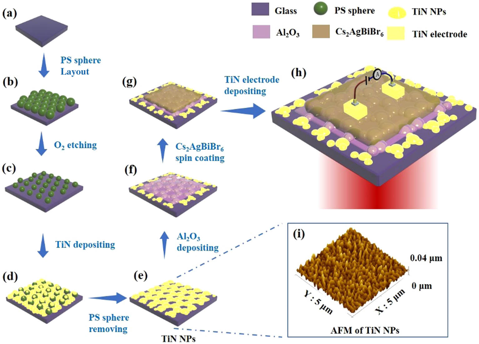
The PS nanosphere self-assembly method together with the reactive-ion etching (RIE) method was utilized to fabricate TiN NP arrays; see Figs. 1(a)–1(e). PS nanosphere arrays were prepared as follows. First, a glass substrate was treated in the piranha solution (4:1 volume ratio, 98% ) for 20 min to make its surface hydrophilic. Next, a hydrophilic glass substrate was placed on top of a heating plate at 60°C. Then, the PS nanosphere (average diameter: 100 nm) solution was injected onto the substrate at a rate of 0.5 mL/min in the first half and 0.25 mL/min in the second half by a peristaltic pump. In this way, a single layer of highly ordered closely packed PS nanospheres was formed on the substrate; its atomic force microscopy (AFM) image is shown in Fig. 5(a) (Appendix A). Next, the RIE was carried out on the closely aligned PS nanosphere layer to reduce the size of the nanospheres. During the RIE process, the oxygen flow rate was 60 sccm, the etching pressure was 5 Pa, and the etching time was 12 min. Consequently, a sparsely distributed PS nanosphere array was obtained in which the diameters of the nanospheres were around 70 nm; see its AFM image in Fig. 5(b). The PS nanosphere array was then employed as the mask for the subsequent preparation of TiN NPs. The TiN layer with a thickness of 40 nm was fabricated by the RF magnetron sputtering method. Owing to the mask shadowing effect, TiN NPs in the shape of semi-ellipsoids were acquired, surrounding the PS nanospheres. Finally, the PS nanospheres were removed by acetone solution. The desired TiN NPs with diverse sizes were eventually formed; the three-dimensional (3D) AFM image is shown in Fig. 1(i).
Figure 1.Schematic flow chart illustrating the fabrication process of the plasmonic perovskite PD incorporated with TiN NPs and ultrathin layer. (a) Preparing a hydrophilic glass substrate; (b) forming a single layer of highly ordered closely packed PS nanospheres on glass substrate obtained by self-assembly method; (c) obtaining sparsely distributed PS nanosphere array by the RIE method; (d) depositing a TiN layer with a thickness of 40 nm by the RF magnetron sputtering method; (e) obtaining TiN NP array on the glass substrate after removing PS spheres; (f) depositing an ultrathin layer on the above formed TiN NPs by ALD; (g) spin coating the thin film on the interfacial layer; and (h) sputtering TiN electrodes with a thickness of 80 nm on using a copper mesh as the mask. In (h), the light is incident on the PD from the glass side. (i) 3D AFM image of the obtained TiN NPs.
The flow chart for manufacturing the MSM-type plasmonic perovskite PD composed of TiN NPs, interfacial layer and , and the two TiN electrodes is shown in Figs. 1(f)–1(h). The ultrathin layer of 1 nm was deposited on the above-formed TiN NPs by the atomic layer deposition (ALD) method. Then, the thin film was spin-coated on the interfacial layer. Finally, TiN electrodes with a thickness of 80 nm were sputtered by using a copper mesh as the mask. The obtained gap between the two electrodes had a length of 220 μm and a width of 20 μm. The light is incident on the PDs from the glass side.
D. Characterization of Perovskite Film and TiN NPs
The X-ray diffraction (XRD) pattern of the prepared film was measured by a diffractometer (Haoyuan Instrument Co., Ltd., DX-2700, China). Photoluminescence (PL) spectrum measurement at room temperature was carried out by a home-built fluorescence spectrometer system using a 405 nm femtosecond laser (Light Conversion, Carbide 5 W, Lithuania) as the excitation light source. Absorption spectra of the film and TiN NPs were obtained by an ultraviolet–visible absorption spectrometer (Cary-5000, Agilent). Morphologies of the film and TiN NPs were characterized by scanning electron microscopy (SEM) (JEOL-IT500, Japan) and AFM (FM-nanoview1000, China).
E. Characterization of PDs
Current–voltage (I–V) and transient photoresponse characteristics of the PDs in dark and under illumination were measured by a semiconductor analyzer (Agilent B1500). For the transient response measurements, the illuminations were supplied using a collimated LED (505 nm, 850 nm, Thorlabs) and laser (Cnilaser, MGL-F-1310 nm and MGL-F-1550 nm), respectively, with the light intensities characterized by a power meter (Ophir NOVA II). For the wavelength-dependent photocurrent response measurement, a xenon lamp (ZOLIX GLORIAX150A) combined with a monochromator (ZOLIX 0mni-λ 3005) was utilized as the illuminator. During I–V measurements, all the PDs were placed on a probe station within a shield box (PRCBE, mini). Noise currents were measured by a lock-in-amplifier (SR865A, Stanford) and a low-noise current preamplifier (SR570, Stanford).
3. RESULTS AND DISCUSSIONS
Figure 2(a) presents the typical SEM image of the surface of the coated film, which shows that the film comprises crystalline grains in sizes of several hundred of nanometers. Figures 6(a)–6(d) (Appendix A) show the SEM images of the coated films when the acceleration speed during spin coating is reduced from 1400 to 800 (r/min)/s. It is found that a moderate acceleration speed of 1000 (r/min)/s can facilitate the formation of perovskite film with high crystalline quality. The AFM image of the sample with the optimal acceleration speed of 1000 (r/min)/s is also displayed in Fig. 7(a) (Appendix A), further verifying its large grain feature in morphology. Here, the surface roughness of the prepared optimal film is 18.57 nm, indicating that the film has a flat surface. Next, the XRD characterization was used to identify the crystalline quality and the structural information of . As shown in Fig. 2(b), there are a series of sharp and intense diffraction peaks in the XRD pattern of the coated film, which are consistent with those previously reported in the literature [13–15]. From the XRD pattern, it is deduced that the product is indeed film of high crystalline quality. Figure 2(c) shows its absorption spectrum, which manifests an absorption peak at 450 nm. From the absorption versus photo energy diagram displayed in Fig. 2(d), its bandgap can be derived, which is about 2.21 eV, corresponding to an absorption band edge of about 560 nm, consistent with the value reported in the literature [31]. At wavelengths below its bandgap, one can also see some weak absorption of light, which could be related to the generation of self-trapped excitons in film [32]. The steady-state PL spectrum of the prepared film is shown in Fig. 2(e), which indicates that the emission peak is located at 625 nm and the corresponding full width at half-maximum (FWHM) is around 120 nm. All these characterizations confirm that the product is film with high crystalline quality, ready for the subsequent demonstration of high-performance PDs.
Figure 2.(a) SEM image; (b) XRD pattern and (c) absorption spectrum of the film; (d) absorption versus photo energy of the film for deriving the bandgap; (e) steady-state PL spectra and (f) measured absorption spectra of the prepared films of and NPs, respectively.
We used an array of sparsely distributed PS nanospheres as the mask to prepare the required TiN NPs, whose 3D AFM image is shown in Fig. 1(i), on top of which a hybrid plasmonic perovskite PD is fabricated (see Section 2.C for fabrication details). It is mentioned that in between the TiN NPs and the film, an atomically thin film is introduced, aimed at promoting the crystallinity of the film. First of all, it is confirmed by the XRD characterization that the film prepared on the surface of modified TiN NPs has crystalline quality that is close to that of the control, which is much better than the film prepared directly on top of the TiN NPs; see Fig. 8 in Appendix A. Figure 2(e) shows the steady-state PL spectra of the samples with or without additional and TiN NPs. It is found that the peak position of the PL emission of the hybrid sample of NPs is almost the same as that of the pristine sample. In comparison with the pristine film, the PL intensity of the NP sample shows an apparent quenching. The quenching in the steady-state PL is attributed to the charge transfer from to TiN NPs, which reduces the intensity of radiative recombination within . Figure 2(f) shows the measured absorption spectra of both the and NP samples. It is seen clearly that in comparison with the pure , an overall increase in absorption in the broadband wavelength range from 500 to 1600 nm is observed for the hybrid sample of NPs. In addition, the hybrid sample possesses a strong absorption peak located at 790 nm, with an absorption efficiency of . Such a characteristic is highly appreciated for boosting the photodetection performance of PDs by the plasmonic hot carrier strategy.
Figure 3(a) compares the dark I–V characteristics of the control PD along with the TiN NPs incorporated plasmonic PD, which also embraces an interfacial layer. Additionally, the dark I–V characteristic of the plasmonic PD comprising and TiN NPs, that is without interfacial, is also characterized for comparison. It is observed that the dark current of the control PD is quite low, reaching 180 fA under 1 V. The very low dark currents must be ascribed to the high crystallinity quality of the as-coated film along with the built Schottky junctions at the interfaces between and the two TiN electrodes. However, after introducing an array of TiN NPs, the plasmonic PD of NPs exhibits a deterioration in dark current (in detail, at 1 V bias it rises by more than 2 orders of magnitude). Such a high dark current is unfavorable for realizing high-performance PDs, especially for the collection of plasmonic hot carriers generated in the NIR region. Because the number of hot carriers transferred into the film is very low, the condition of high dark current would easily result in the low amplitude of the hot carrier signal being submerged in the background noise. The increased dark current might be due to a less favorable film morphology and lower crystallinity of the coated film directly prepared on top of TiN NPs; see Fig. 8(b). It was reported that introducing a thin layer could promote the formation of high-quality perovskite films and suppress the dark current of the PDs [9,33]. Therefore, we added an atomically thin layer (see Section 2.C for PD fabrication details) in order to cover the TiN NPs array, prior to spin coating the film. It is found in Fig. 3(a) that with the assistance of the interfacial layer, the dark current of the plasmonic PD is reduced significantly with respect to the plasmonic PD comprising NPs. Eventually, the dark current of the hybrid NP device can be maintained at a low level (700 fA at 1 V), which is quite close to that of the control PD. This improvement arises from the relatively good crystalline quality of the film, improved with the help of the atomically thin interlayer; see Fig. 8(a).
Figure 3.(a) I–V curves of , NPs, and NP devices measured in the dark. (b) and (c) I–V curves of the , NP, and NP devices under 505 and 850 nm light illuminations. Insets, transient photocurrent responses of the and NP devices at 505 and 850 nm, respectively; (d) transient photocurrent curves of the device and NP device at 505 and 850 nm; (e) LDR characterization of the NP device measured under 505 and 850 nm illuminations at 1 V; (f)–(h) EQE, R, and of the and NP devices at different wavelengths; (i) measured noise currents of the and NP devices at various frequencies at 1 V bias. The calculated shot noise and thermal noise limits are also included for reference.
Figures 3(b) and 3(c) show the I–V characteristics of the three types of PDs, , NPs, and NPs, measured under, respectively, 505 and 850 nm light illumination at a power density of . It is seen that, under 505 nm light illumination, the photocurrent of the device at 1 V is the lowest among the three devices. Relative to the control, the photocurrent of the NP device is significantly enhanced, and its enhancement is more obvious compared with that of the NP device. The photocurrent characteristics of the three types of PDs under 850 nm illumination follow the same rule. Such a difference between the two plasmonic devices comes from the difference taking place in the film qualities of the films prepared on different surfaces. The relatively poor crystalline quality grains obtained in the NP device degrade the transportation of carriers through , resulting in the suppression in the photocurrent. The calculation indicates that the corresponding photo-to-dark current ratio of the NP plasmonic device at 1 V under 505 nm illumination reaches , close to that of the device (). Surprisingly, the photo-to-dark current ratio of the NP plasmonic device at 1 V under 850 nm illumination reaches 43, much greater than that of the device (1.20). For the NP device, because its dark current is over-large, its photo-to-dark current ratio is very small; this kind of device will be excluded in the following discussion. The insets of Figs. 3(b) and 3(c) show the transient photocurrent responses of the and the NP devices at 505 and 850 nm, respectively. Clearly, with the synergetic impacts from the TiN NPs and , the hybrid device exhibits much improved photocurrent responses with respect to the control at 505 nm wavelength. Most importantly, the transient photocurrent response of the control PD at 850 nm comes closest to a straight line, verifying that it fails to respond to the incidence; in contrast, the plasmonic PD manifests an apparent on–off electric signal change following the variation of the incidence.
Figure 9 in Appendix A plots the transient photocurrent characteristic of the and the NP devices at 505 and 850 nm after being switched on and off multiple times. It shows that the devices can respond stably with the change of the light signals. The response time of the devices was measured by a single representative light/dark cycle at 505 and 850 nm. As derived from Fig. 3(d), the rising time (from 10% to 90% of the saturated value) and falling time (from 90% to 10% of the peak value) for the device at 505 nm are 1.2 and 2 ms, respectively, comparable to other planar photodetectors [34]. After introducing TiN NPs, the rising and falling times are 3.8 and 0.5 ms, respectively. We also measured the response time for the NP device at 850 nm. The rising and falling times are 1.5 and 3.9 ms, respectively. Photocurrents of the NPs at different light intensities of 532 and 850 nm measured at 1 V bias are presented in Fig. 3(e). As the light intensity increases at 505 nm, photocurrent increases linearly in the range from to , which corresponds to an LDR of 126 dB. As the light intensity increases at 850 nm, the photocurrent increases linearly in the range from to , which corresponds to an LDR of 106 dB. Meanwhile, we characterized photocurrents of the device at different light intensities of 532 nm (Fig. 10 in Appendix A). The LDR for the control device at 505 nm is 124 dB. The LDR calculation is given in Eq. (B5). We further characterized the photocurrent responses of the and NPs devices in the longer than 850 nm wavelength region with the power density fixed to . The I–V characteristics measured at 1310 and 1550 nm illuminations are picked up as examples, as shown in Figs. 11(a) (control) and 11(b) ( NPs) in Appendix A, respectively, in which the individual dark I–V curves are also included. It comes out that the photo-to-dark current ratios of the NP device are 7.5 and 5.5 at 1310 and 1550 nm, respectively, while the control device shows no distinction between photocurrents and dark currents under various biases at the two wavelengths. These experimental results demonstrate that the NP device is much superior to the control device in detecting NIR light.
According to the I–V measurement results at different wavelengths, the EQEs for the and NP devices at different wavelengths can be calculated, as displayed in Fig. 3(f). The EQE is calculated according to Eq. (B4). Because the control device does not respond to the light at wavelengths of 980, 1310, and 1550 nm, the corresponding EQEs are not calculated. It is witnessed that the NP device displays enhanced EQE values relative to the device over a broadband wavelength range. Within the intrinsic absorption band of the film, e.g., at 375 nm, the increase in EQE by NP incorporation is not observed, because the TiN NPs block part of the incidence. At the 505 nm wavelength, which is close to the absorption edge of , the enhancement in EQE becomes significant by NP incorporation, with its EQE increasing from 126% to 361%, corresponding to an enhancement factor of 186%. Evidently, the EQE enhancement factors of NP device with respect to the control are enormously great at wavelengths beyond the absorption band of . For example, at 850 nm wavelength, the EQE of the control PD is only , revealing the pretty weak generation of photocarriers within ; by comparison, the EQE of the plasmonic perovskite PD reaches about 0.56%, corresponding to an enhancement factor of around 2332. According to EQE measurements, responsivity of the device and the NP device can be derived, as shown in Fig. 3(g). At 505, 850, and 1550 nm, the responsivity of the plasmonic PD is 1.47 A/W, 3.8 mA/W, and 0.8 mA/W, respectively. The responsivity at 505 nm is times larger than that of the control device (0.5 A/W). For characterizing the detectivity, we directly recorded their noise currents experimentally (see Section 2.E), as displayed in Fig. 3(i). Both the noise currents for the device and NP device are very low, and they are very close to the shot noise (ins) and thermal noise (int). The relevant calculation details can be found in Eqs. (B1) and (B2). Based on the measured EQE and noise current, of the control and plasmonic devices can be obtained, as shown in Fig. 3(h). is calculated according to Eq. (B3). It is found that in the NIR region, of the plasmonic PD at 850 nm can reach a level above Jones.
By examining the enhancement factors in measured absorption of the and the NP films as shown in Fig. 4(a), one notices strong coincidences in the tendency between the EQE and absorption enhancement at varied wavelengths. It should be noted that in the wavelength range of the intrinsic absorption band, the absorption enhancement factor is low because the absorption of the control device is high. In contrast, the absorption enhancement at the NIR region is quite high because the reference absorption is low. The relatively higher enhancement factors in absorption than those in EQE illustrate that the photo-to-electric conversion process inevitably suffers additional loss during the processes of carrier transportation and collection. Here, it is mentioned because we use discrete laser components as the illumination sources during EQE spectrum measurement. This enhancement peaks in absorption spectra at 790 nm cannot be exactly reproduced in the EQE enhancement spectrum. Overall, it is reasonable to infer that the enhancement of photocurrent at the NIR region originates from the enhanced absorption caused by localized plasmonic resonances excited by the TiN NPs.
Figure 4.(a) EQE and absorption enhancement factors at different wavelengths; (b) simulated absorption spectra of the and NP structures; (c) electric field distributions in the plane at the simulated absorption peak of 735 nm for the NP structure; (d) contact potential map of the modified TiN NPs taken by the KPFM technique ( and are the average contact potential and work function of the modified TiN NPs, respectively); (e) energy band diagram of the NP device (, , , ); (f) working mechanism of the NP device, illustrating hot hole excitation and transfer driven by plasmonic resonances.
In order to further reveal the mechanism of the above-observed broadband absorption enhancement in film by incorporating TiN NPs, we carry out the electromagnetic simulation (see Appendix B.2 for simulation details). According to the 3D AFM image of the utilized TiN NPs [Fig. 1(i)], we know that the TiN NPs are particles in the shape of a semi-ellipsoid. The particle sizes of TiN NPs are accurately evaluated statistically, and the corresponding results are shown in Fig. 12(a) (Appendix A). According to the geometries of acquired TiN NPs, a simplified structure with compound TiN NPs distributed within one unit cell [Fig. 12(b)] is simulated. It is noted that in simulation, the 1 nm thick layer is neglected because it does not cause any noticeable change in absorption efficiency [2]. Figure 4(b) shows the simulated absorption spectra of, respectively, and NP structures. A comparison between the measured and simulated absorption spectra of the NPs can be found in Fig. 12(c). It is witnessed that the NP device exhibits improved absorption in the broadband wavelength range from 500 to 1600 nm, roughly consistent with the experimental results. The difference in the position and amplitude of the absorption peak between simulation and experiment is acceptable because, in reality, the TiN NPs are diverse in size, and their shapes also deviate from the perfect semi-ellipsoid. Figure 4(c) plots the electric field distribution in the plane at the simulated absorption peak of 735 nm for the NP structure, and the electric field distributions at multiple planes are also displayed in Fig. 12(d). It is observed that there are not only dipole-like plasmonic resonances excited by individual TiN NPs, but also those close packaged NPs have strong interactions with each other, so that some strong electric fields are also excited at the extreme narrow gaps. The electric field distributions in the plane at the simulated absorption peaks of 555 and 1145 nm are also plotted in Figs. 12(e) and 12(f). At different wavelengths, the electric field enhancements take place at different regions. Especially, at the NIR wavelength of 1145 nm, there are two NPs displaying quite strong interactions with quite strong electric field located at the gap in between them. Moreover, it is because the TiN NPs vary in size and shape so that the absorption of NP film can absorb light over a broadband wavelength range covering both visible and NIR regions.
At the wavelength close to the absorption edge (e.g., 505 nm), the photocurrent enhancement originates from the enhanced absorption taking place in perovskite produced by localized plasmonic resonance of TiN NPs [23]. In the following, we focus on explaining the contribution from TiN NPs to detecting light at NIR regions where the barely absorbs light. After the NIR light is absorbed by TiN NPs, plasmonic hot carriers can be generated, causing the subsequent enhancement in EQE of PDs. Thus, the energy band diagram should be analyzed to reveal the mechanism of the plasmonic hot carrier in the proposed PD. The work functions of the TiN NPs and the can be evaluated by the Kelvin probe force microscopy (KPFM) technique. According to the measured contact potential maps of the modified TiN NPs and the surfaces shown in Fig. 4(d) and Fig. 7(b), the work functions of average modified TiN NPs and are about 4.92 and 5.16 eV, respectively. Here, the contact potential map of the reference highly oriented pyrolytic graphite (HOPG) sample is also shown in Fig. 13 (Appendix A), and the calculation method for the work function is given in Eq. (B6). The energy levels of the bottom conduction band () and top valence band () of are located at and , respectively. The Fermi level () of is characterized to be by the KPFM method, indicating that the prepared is a weak p-type semiconductor. Accordingly, the energy band diagram of the NP device can be drawn, as shown in Fig. 4(e). Here, a Schottky junction is formed at the interface between and the modified TiN NPs. The height of the Schottky barrier () at the interface can be calculated using the following equation [35]: , where is the work function of TiN NPs. When TiN NPs efficiently absorb NIR light, it produces a large number of hot holes, among which those with photo energies greater than have the possibilities to flow from TiN NPs into the valence band of , consequently contributing to the significantly improved EQEs as shown in Fig. 3(f). Here, is calculated to be 0.78 eV, which means that the energy of the hot holes must be greater than 0.78 eV to enter the . The incident photon with energy of 0.78 eV has a wavelength equal to 1590 nm. That justifies why the proposed plasmonic NP device can respond to telecommunication light (1550 nm). Here, TiN NPs are adopted because the work function of TiN is close to that of the ; thereby, the built Schottky junction has a low barrier height, which facilitates the transfer of hot holes from TiN to . By comparison, although metal NPs made of Ag, copper (Cu), and aluminum (Al) can also excite plasmonic resonances, their relatively low work functions render an increased Schottky barrier, which adversely impacts the hot hole injection at long wavelengths. The work function of Au is also close to that of the . However, the cost of Au is high.
Figure 5.Atomic force microscopy (AFM) image of the (a) monolayer polystyrene (PS) spheres and (b) sparsely-distributed PS nanosphere array.
Figure 6.SEM images of films prepared at the acceleration speed of (a) 1400 (r/min)/s, (b) 1200 (r/min)/s, (c) 1000 (r/min)/s, and (d) 800 (r/min)/s, respectively.
Figure 9.Transient photocurrent characteristic of the devices switched on and off multiple times at a power density of : (a) the device at 505 nm, (b) the NPs device at 505 nm, (c) the NPs device at 850 nm.
Figure 12.(a) Particle size distributions of the TiN NPs. (b) Structure of the NPs device utilized in simulation. (c) Measured and simulated absorption spectra of the NPs structure. (d) Electric field distributions at multiple planes at the simulated absorption peak of 735 nm. (e), (f) Electric field distributions in the plane at the simulated absorption peaks of (e) 555 nm and (f) 1145 nm.
Figure 13.Contact potential map of the reference highly oriented pyrolytic graphite (HOPG) sample taken by the KPFM technique ( and are the average contact potential and work function of the HOPG, respectively).
In conclusion, we have introduced TiN NPs, by the low-cost PS nanosphere self-assembly method, into the lead-free PD, to realize the broadening of the response band. After incorporation of TiN NPs, the photocurrent has been increased over a broadband wavelength range from 505 to 1550 nm. At the same time, the dark current has been maintained at the same level of the control device by introduction of a thin layer. The photocurrent enhancement in the absorption range of originates from the enhanced absorption taking place in perovskite produced by the localized plasmonic resonance of TiN NPs. The photocurrent enhancement at long wavelengths beyond the light absorption range is attributed to the generation of hot holes within TiN NPs and the collection of those hot holes. The photocurrent enhancement factors in the long wavelength range reach above 2000. It is worth noting that by incorporating TiN NPs, the photocurrent response of the PD overcomes the wavelength limit imposed by the absorption of perovskite, and extends to the telecommunication band of 1550 nm. This work provides an alternative strategy for achieving environmentally friendly and broadband perovskite PDs.
APPENDIX A
Figure 5 shows the AFM images of the closely packed PS spheres and sparsely-distributed PS nanospheres after etching. Figure 6 displays the SEM images of the films prepared at different acceleration speeds. Figure 7 shows the 3D AFM and KPFM images of the film, respectively. Figure 8 shows the XRD patterns of the films prepared on top of TiN NPs with and without interfacial layer. Figure 9 exhibits the transient photocurrent curves of the devices under the condition of being switched on and off multiple times. Figure 10 shows the LDR characterization of the device under 505 nm LED illumination. Figure 11 represents the I-V curves of the and the //TiN NPs devices measured in dark and under illumination. Figure 12 includes the particle size distributions of the TiN NPs, structure of the /TiN NPs in simulation, measured and simulated absorption spectra, and electric field distributions at different wavelengths. Figure 13 shows the contact potential map of the reference HOPG sample.
APPENDIX B
Calculations
Noise current () is a significant factor evaluating the sensitivity of photodetectors. The two main noise sources are the shot noise () and the thermal noise (), respectively. The shot noise () can be calculated from the dark current () using the following equation: where is the dark current, is the elementary charge, and is the electrical bandwidth, based on dark current of the device at 1 V bias. Besides the shot noise, the thermal noise () is determined by the following equation: where is the Boltzmann constant, is the temperature, and is the resistance of the device. Based on the dark current curve, the resistance at 1 V is obtained.
Based on directly recording their , the of the PD is deduced by the following equation: where is the active area of the devices. The corresponding can be calculated from the EQE using the following equation: where is Planck’s constant, is the velocity of light, is the electron charge, and is the wavelength of incident light.
The LDR of the devices could be deduced by the following equation: where and are the maximum and minimum incident light intensities in the linear response range.
The work functions of the films could be deduced by the following equation: where is the absolute value of the charge of the electron, is the work function of the tested sample, is the work function of HOPG (with a fixed value of 4.65 eV), and and are the average contact potentials of the sample and HOPG obtained from the KPFM images. The surface Fermi level is equal to the work function in amplitude, but the sign is opposite.
Simulations
In simulation, we simplify the acquired TiN NPs with diverse sizes into a periodic TiN NP structure, with the schematic diagram in simulation as shown in Figure 7(b). The calculations are carried out assuming a periodic boundary along the and axes. The thicknesses of perovskite and are 300 and 500 nm, respectively. The geometry of the TiN NPs array consists of two different shapes of semi-ellipsoids: a large semi-ellipsoid with a long axis of 52 nm, a short axis of 40 nm, and a height of 40 nm; and a small semi-ellipsoid with a long axis of 48 nm, a short axis of 36 nm, and a height of 30 nm. Perfectly matched layer (PML) boundaries are applied to the top surfaces. Light is illuminated from the bottom to the TiN NPs. The wavelength-dependent refractive indices and extinction coefficients of all materials utilized in simulation were acquired through the ellipsometry method.
[31] G. Liu, Z. Zhang, C. Wu. Extending absorption of Cs2AgBiBr6 to near-infrared region (≈1350 nm) with intermediate band. Adv. Funct. Mater., 32, 2109891(2021).
 AI Video Guide
  AI Picture Guide
 AI One Sentence