
Aroutin Khachaturian, Reza Fatemi, Artsroun Darbinian, Ali Hajimiri, "Discretization of annular-ring diffraction pattern for large-scale photonics beamforming," Photonics Res. 10, 1177 (2022)
- Photonics Research
- Vol. 10, Issue 5, 1177 (2022)
Abstract
1. INTRODUCTION
Integrated solid-state photonic beamformers (optical phased arrays, or OPAs) have the potential to reduce the cost, size, and implementation complexity of many photonic systems compared to their bulk optics and micro-electromechanical systems (MEMS) counterparts [1,2]. These solid-state beamformers have been recently demonstrated for lidar [3,4], photonic beam steering [5–7], medical imaging [8], and remote sensing [9] applications. In particular, standard silicon photonics processes can further reduce the cost and increase the yield and reliability of such systems [6,10–12]. However, there are several challenges associated with the realization of large-scale, solid-state beamformers.
Most integrated photonic dielectric waveguides and radiators have a minimum size and spacing on the order of the wavelength. Any 2D aperture constructed with uniformly spaced radiators will require a large inter-element spacing to route the signals to the inner elements of the array. This leads to minimum pitch and spacing constraints that then lead to a reduced field of view (FOV) and increased grating lobes as the size of the array aperture increases. There are two categories of architectures that have been used to overcome this problem. One class of architectures uses a wavelength-sensitive 1D grid array of radiating elements to steer the beam in one direction and sweep the wavelength of the laser to steer the beam in the perpendicular direction [10,11,13–15]. This method removes the planar routing restriction at the cost of an increased laser source and system complexity. Typically, a broadly tunable laser source (around 100 nm of wavelength tunability) is required to achieve a moderate FOV (around 20°) [10,14,16]. Such tunable lasers are more complex and hence more costly compared to their single wavelength counterparts. Furthermore, such OPAs cannot offer wavefront control in the steering direction controlled by the wavelength.
Another class of architectures uses sparse array synthesis techniques to construct a 2D grid array of radiating elements that permit routing the signals of the inner elements of the array [6]. Compared to their equal-sized aperture, half-wavelength spacing counterparts, sparse arrays reduce the number of the radiating elements and phase shifters required, thus reducing array control complexity, power consumption, heat dissipation, and system cost. Furthermore, such arrays can operate with a fixed-wavelength laser source. These 2D grid OPAs have advantages over their 1D grid aperture counterparts since they can offer full wavefront control with a fixed wavelength laser. However, sparse placement of the elements reduces the array gain and beam efficiency, which is also known as the “sparse array curse.” This fact fundamentally limits the performance of sparse arrays for power transfer applications, making them more suitable for point-by-point imaging and sparse target detection applications. Furthermore, most sparse array synthesis techniques achieve target beam performance by the randomized placement of elements in a 2D grid given the constraints on the number of elements and planar signal routing. For example, genetic algorithms have been used for sparse array synthesis [6,17,18]. This optimization process is computationally expensive for larger aperture sizes with an increased number of elements and there is no guarantee of arriving at the optimal design.
Sign up for Photonics Research TOC. Get the latest issue of Photonics Research delivered right to you!Sign up now
One method to reduce the complexity of finding optimum sparse apertures is to take advantage of the basic properties of circularly symmetric apertures. The ideal symmetric aperture is circular, as shown in Fig. 1(a). The beam pattern of such an aperture can be computed by taking the Fourier transform of a circle:
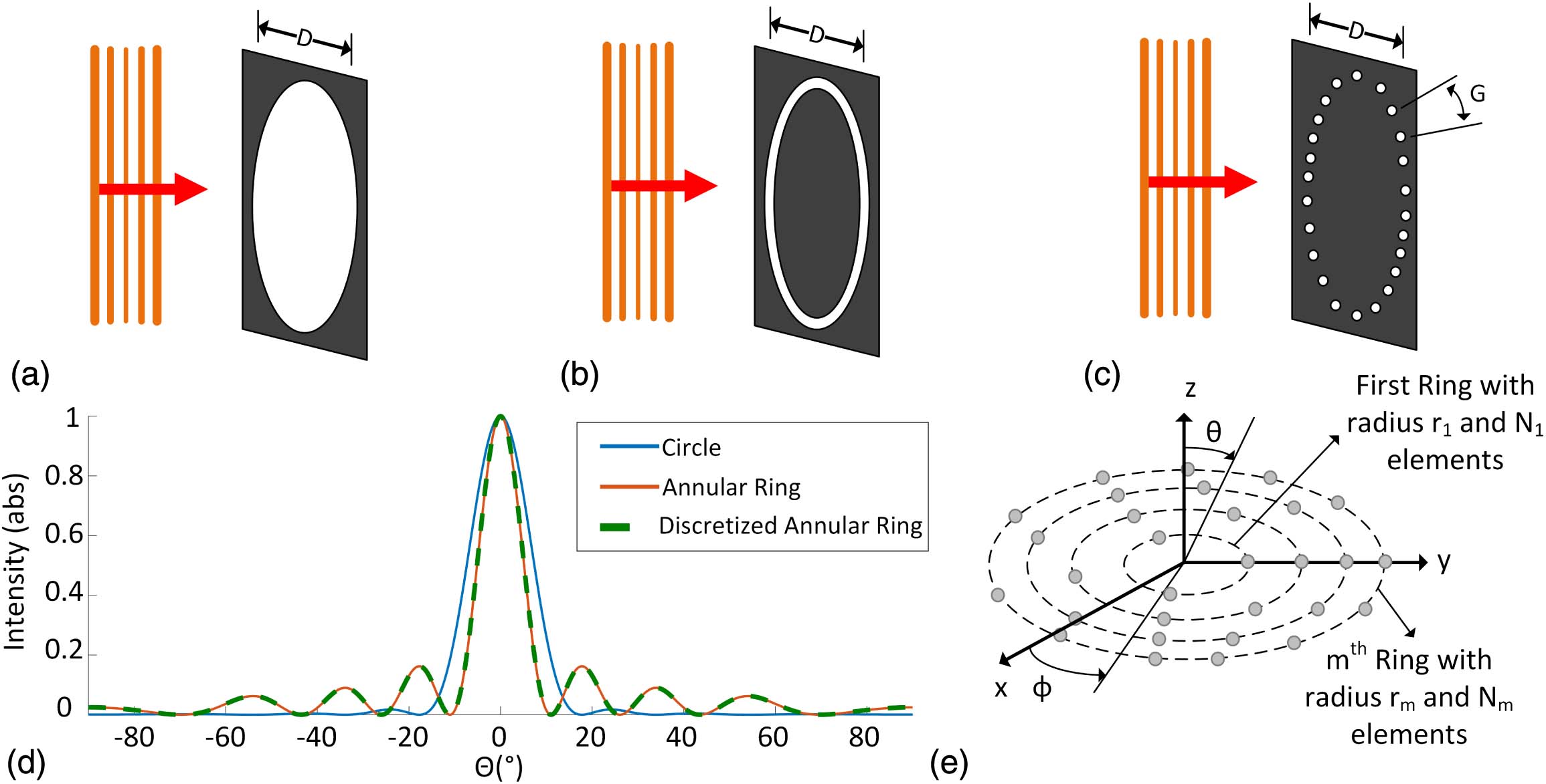
Figure 1.Diffraction pattern of circularly symmetric apertures with diameter
These beam patterns show that annular-ring apertures reduce the beamwidth at the cost of an increased side-lobe level (SLL) compared to their circular counterparts that have an aperture with a significantly larger area. More importantly, annular-ring apertures do not produce grating lobes. This annular-ring aperture can be realized in a planar photonics process. We can physically implement an OPA capable of active beam steering by placing radiating elements on this annular ring at half-wavelength spacing, as shown in Fig. 1(c). This discretized annular-ring array pattern approximates to the pattern of a continuous annular-ring aperture, which is shown in Fig. 1(d), for a sufficiently large number of elements. It is possible to combine multiple such discretized annular rings to improve the OPA beamwidth and SLL, as shown in Fig. 1(e). In phased array theory, such multi-annular-ring apertures can be categorized under circular-aperture arrays [19–24]. The theoretical performance of uniform and nonuniform circular arrays and their application to an integrated OPA have been previously analyzed and discussed in Refs. [21,25]. Such symmetric apertures are advantageous over their rectangular counterparts since they exhibit minimal disturbance to the beamwidth and SLL when scanned azimuthally over the entire plane [26].
In this paper, we demonstrate what we believe, to the best of our knowledge, is the first implementation of such multi-annular-ring OPAs in a silicon photonics process and analyze the architectural advantages and the limitations of such OPAs. In the next section, we analyze the beamforming characteristics of such annular rings in the context of planar photonics platforms. Afterward, we present a 255-element silicon photonics implementation of such an annular-ring OPA transmitter with full amplitude and phase control for individual radiators. This OPA design can be modified to operate as a transceiver [27] or as a heterodyne receiver by incorporating balanced detectors [6]. We simplify the electrical drive interconnect complexity of such an OPA by using a row–column drive that reduces the total number of electrical interconnects from 510 nodes to 100 nodes. Finally, we discuss the beamforming optimization methodology of this large-scale OPA and demonstrate the beamforming and beam-steering capability of this OPA.
2. ANALYSIS OF ANNULAR-RING APERTURES
The discretized multi-annular-ring aperture can be generalized by creating
A. Approximation of Continuous Annular-Ring Aperture
Using Eq. (3), we can compute the diffraction pattern of the continuous annular-ring aperture in Fig. 1(b) by assuming
As shown in Fig. 1(d), placing discretized elements at distances up to half-wavelength spacing is equivalent to the continuous case with a Bessel function beam pattern for the entire FOV. As a result, the beam pattern of this circularly symmetric structure is independent of
![]()
Figure 2.(a) Effect of annular-ring discretization on the far-field array factor. A 20 μm diameter ring is plotted for a continuous annular-ring-slit aperture (or half wavelength-spacing elements), discretized with 40 isotropic radiators and 20 isotropic radiators. (b) Beamwidth and 3 dB beam efficiency trends as a function of phased array aperture diameter. (c) Minimum beamwidth as a function of 3 dB beam efficiency for linear density multi-annular-ring OPAs at the planar routing limits for single-layer and two-layer photonics process. (d) SLL and effective aperture as a function of aperture diameter.
B. Annular-Ring Apertures with a Fixed Linear Density
This multi-annular-ring aperture given by Eq. (3) is circularly symmetric, and as a result, the placement of the radiating elements can be optimized for desired performance parameters with reduced computational complexity compared to their rectangular grid sparse apertures counterpart. Such multi-annular-ring apertures can be analyzed for any of the beamforming parameters such as beamwidth, SLL, beam efficiency (defined as the ratio of the optical power in the 3 dB beamwidth of the main lobe and the total power delivered to the aperture), and element count. In this work, we limit our analysis of annular-ring apertures to apertures with fixed linear density. In other words, we assume a constant elements per arc length density (
For such apertures with linear density, the planar photonic process parameters set the elements per arc length density as well as the minimum aperture diameter limits. For silicon photonics processes, the waveguides are typically 500 nm wide with a minimum pitch of 1 μm to reduce the electromagnetic coupling between the adjacent waveguides. Radiating elements can also be constructed at the size of the waveguides (500 nm). For a fixed linear density, the design values
Figure 2(c) demonstrates the general trade-off between beam efficiency and minimum beamwidth, which is limited by the “sparse array curse.” Nevertheless, the aperture efficiency can be moderately improved by using various array-synthesis techniques such as fine-tuning the position of the radiating elements inside the aperture or incorporating amplitude apodization. For example, a multi-annular-ring array with
3. MULTI-ANNULAR-RING OPA IMPLEMENTATION
To demonstrate the beamforming and beam-steering capability of multi-annular-ring aperture OPAs, we implemented a five-annular-ring aperture OPA system with active beamforming in Advanced Micro Foundry’s (AMF) standard photonics process. The die photo of this system is shown in Fig. 3. This OPA has a 400 μm diameter annular-ring aperture with 255 radiating elements with complete phase and amplitude control. The thermo-optic phase and amplitude modulators are distributed into four blocks and electrically connected in a row–column fashion to reduce the electrical interconnect density from order
![]()
Figure 3.Multi-annular-ring aperture OPA system. Die photo of the proposed design and SEM photo of the aperture. Phase and amplitude modulators are grouped into four blocks for symmetric layout.
A. Implemented Aperture
This multi-annular-ring OPA array factor was optimized based on a 1 μm minimum pitch in the waveguide routing with
![]()
Figure 4.(a) Layout and signal distribution for a 255-element annular-ring aperture. (b) Full AF of the aperture for
The radiating element used in this aperture has a 3 dB far-field beamwidth of
B. Row–Column Drive
The amplitude and phase modulators for the 255-element array are divided into four blocks. Both amplitude and phase modulators incorporate a compact spiral thermo-optic phase shifter design to reduce the device footprint and increase isolation between radiating elements [29], as shown in Figs. 5(b) and 5(c). The amplitude modulation is achieved by a cascade of tunable optical couplers that split the light into 64 branches. This tunable power splitter requires 63 tunable couplers. The output of each tunable coupler passes through phase shifters before reaching the radiating elements to adjust the relative phase between elements. These 127 active components are electrically connected in a row–column fashion, as shown in Fig. 5(a). The tunable couplers are arranged in a
![]()
Figure 5.Row–column drive scheme for amplitude and phase modulators. (a) Four out of 16 rows from the
To achieve independent control of all phase and amplitude modulators, each of these four blocks is programmed by a time-domain demultiplexing technique that uses the thermal memory of these phase shifters. In this scheme, the modulators are programmed in continuous cycles. Each programming cycle,
This row–column drive methodology trades the number of required drivers and system complexity with an increased requirement on driver bandwidth, output voltage swing, and drive signal complexity. Scaling the total number of phase and amplitude modulators by a factor of
C. Amplitude Modulation with Simplified On-Chip Calibration
Amplitude modulation for the 255 elements in this design is achieved by cascading 8 one to two tunable optical couplers [Fig. 6(a)]. This design is advantageous over the conventional approach of dedicating one amplitude attenuator per signal path [27] because, for different amplitude configurations, the power is redistributed between different paths, and the total power delivered to the aperture remains constant. This distribution method can be used to deliver equal power to all elements or to achieve amplitude apodization for reduced SLL. Each output of these amplitude modulators has a 1% power splitter and a compact sniffer photodetector for on-chip calibration. The output of these photodiodes can be used to perform a one-time calibration to correct for fabrication mismatches in the tunable amplitude coupler and determine the drive voltage requirement for the amplitude modulators.
![]()
Figure 6.Tunable amplitude modulation with calibration feedback. (a) Unit tunable power splitter with 1% sniffer output for control. (b)
It can be noted that this calibration requires
In this OPA system implementation, the power is coupled into the aperture using a lensed grating coupler. An integrated PIN modulator isolates the coupled light from the scattered reflected light from the substrate. Integrated proportional-to-absolute temperature (PTAT) sensors can be used to measure the substrate temperature gradient across the chip. The optical path-length mismatch between radiating elements is compensated for by incorporating additional delay lines in the chip. The entire system has a
4. MEASUREMENT RESULT
The amplitude and phase modulator unit cell with the compact spiral phase shifters was characterized in Ref. [29]. These modulators have a 19 kHz electro-optical bandwidth and require 21.2 mW for a
The far-field radiation pattern of the OPA was captured using a custom optical far-field radiation measurement setup. This apparatus moves a compact InGaAs photodetector along the arc at a fixed distance with respect to the OPA chip and captures the far-field pattern point by point. The 1.55 μm light coupled into the chip is modulated at 1.1 MHz by the integrated on-chip PIN modulator. Therefore, the modulated optical power radiated from the aperture can be distinguished from the scattered light at the input grating coupler (due to fiber-to-chip coupling inefficiencies). Note that the on-chip PIN modulation frequency can be set to any value as long as it is within the electrical bandwidth limitations of the far-field measurement setup. This transmitter path modulation is compatible with time-domain encoding schemes such as FMCW and receiver architectures such as heterodyne receivers [6]. Furthermore, no interference between this transmitter path modulation and the drivers and phase shifters in the row–column drive scheme was observed during far-field beam optimization and characterization measurements. The far-field radiation power was filtered and quantized using a spectrum analyzer with 10 Hz resolution bandwidth. The collected power was normalized with respect to the power coupled into the chip to remove any changes in power due to the slight variations in the position of the input fiber during the measurement.
All of the phase and amplitude modulators in the array were optimized concurrently using the 36 PAM drivers. These PAM drivers switch between 16 different values with 10-bit resolution for the 16 different rows. During each iteration of beam optimization, the algorithm must optimize all the phase and amplitude modulators in each of the four
![]()
Figure 7.(a) Beam power optimization progression after 450 iterations. (b) Dynamic stability and repeatability of the annular-ring OPA. The PAM drivers can maintain the optimized setting with less than 0.4 dB variations.
To verify the dynamic beamforming stability and repeatability of this OPA, we switched between the setting with all PAM drivers off and the optimum PAM setting for the broadside and recorded the dynamic changes in the normalized main beam power (with respect to the power coupled into the chip) as a function of time. The dynamic stability of the PAM drive is shown in Fig. 7(b). It takes 2 s to program the 576 values into the 32 PAM drivers. The thermal gradient variations on the chip settle in approximately 8 s, which is the limiting factor for the total optimization time per beam direction. This thermal settling time is a function of the particular measurement setup and can be reduced by improving the substrate heat sink. The PAM drivers are able to consistently program the phase and amplitude modulators through the row–column drive scheme with less than 0.4 dB ripple in the peak power.
Afterward, we measured the optimized beam pattern using the aforementioned optical far-field measurement setup. The InGaAs photodetector was rotated along the arc in
![]()
Figure 8.2D beamforming demonstration. (a) 2D beam pattern was measured for the optimized direction (0°, 0°). (b) 1D cross-sections of the beam pattern in
![]()
Figure 9.Cross-sectional view of the beam pattern for several directions. (a) Phase-shifter-enabled beam steering in
5. CONCLUSION
In this work, we analyzed the advantages and design trade-offs of fixed linear density multi-annular-ring-aperture OPAs. Such OPAs reduce the sparse array design complexity due to their symmetric nature and permit signal distribution in a planar photonics process. Furthermore, the linear density of the elements in the OPA maintains a constant power efficiency for larger apertures, reducing the beamwidth and the SLL. In a standard photonics process, we implemented an annular-ring aperture with 255 radiating elements and 510 phase and amplitude modulators. The performance of the proposed 2D aperture multi-annular-ring OPA is compared to other recent 2D aperture OPAs in Table 1. The proposed design uses a row–column drive, which reduces the electrical interconnect complexity from
Comparison of Recent 2D Aperture OPAs
| This | Caltech | Caltech | USC 2015 | UPenn | KIAST | NUAA | |
|---|---|---|---|---|---|---|---|
| Aperture Type | Uniform polar | Sparse Cartesian | Uniform Cartesian | Uniform Cartesian | Uniform Cartesian | Uniform Cartesian, MEMS | Nonuniform polar |
| Number of Radiators (N) | 255 | 128 | 73 | ||||
| Beamwidth | 1° | 0.8° | 0.75° | 0.45° | N/A | N/A | |
| SLL | N/A | ||||||
| Steering Range | 16° | 8° | 1.6° | 7° | 30° | ||
| Number of Maximum Resolvable Spots (S) | 9315 | 400 | 113 | 12 | N/A | 25,600 | N/A |
| Number of Drivers | 100 | 32 | 64 | 129 | 16 | N/A | N/A |
Simulated beamwidth and SLL are 0.2° and
N/A: data not reported in the corresponding publication.
Based on simulation result.
Acknowledgment
Acknowledgment. The authors would like to acknowledge Behrooz Abiri and Parham Porsandeh Khial for their valuable inputs in the design and analysis of this work.
References
[1] A. Tuantranont, V. Bright, J. Zhang, W. Zhang, J. Neff, Y. Lee. Optical beam steering using MEMS-controllable microlens array. Sens. Actuators A Phys., 91, 363-372(2001).
[2] Y. Wang, G. Zhou, X. Zhang, K. Kwon, P.-A. Blanche, N. Triesault, K. S. Yu, M. C. Wu. 2D broadband beamsteering with large-scale MEMS optical phased array. Optica, 6, 557-562(2019).
[3] F. Aflatouni, B. Abiri, A. Rekhi, A. Hajimiri. Nanophotonic coherent imager. Opt. Express, 23, 5117-5125(2015).
[4] S. Chung, M. Nakai, S. Idres, Y. Ni, H. Hashemi. Optical phased-array FMCW lidar with on-chip calibration. IEEE International Solid-State Circuits Conference (ISSCC), 64, 286-288(2021).
[5] F. Aflatouni, B. Abiri, A. Rekhi, A. Hajimiri. Nanophotonic projection system. Opt. Express, 23, 21012-21022(2015).
[6] R. Fatemi, B. Abiri, A. Hajimiri. An 8 × 8 heterodyne lens-less OPA camera. Conference on Lasers and Electro-Optics, JW2A.9(2017).
[7] F. Ashtiani, F. Aflatouni.
[8] M. S. Eggleston, F. Pardo, C. Bolle, B. Farah, N. Fontaine, H. Safar, M. Cappuzzo, C. Pollock, D. J. Bishop, M. P. Earnshaw. 90 dB sensitivity in a chip-scale swept-source optical coherence tomography system. Conference on Lasers and Electro-Optics, JTh5C.8(2018).
[9] A. White, P. Khial, F. Salehi, B. Hassibi, A. Hajimiri. A silicon photonics computational lensless active-flat-optics imaging system. Sci. Rep., 10, 1689(2020).
[10] C. V. Poulton, M. J. Byrd, P. Russo, E. Timurdogan, M. Khandaker, D. Vermeulen, M. R. Watts. Long-range LiDAR and free-space data communication with high-performance optical phased arrays. IEEE J. Sel. Top. Quantum Electron., 25, 7700108(2019).
[11] S. A. Miller, C. T. Phare, Y.-C. Chang, X. Ji, O. A. J. Gordillo, A. Mohanty, S. P. Roberts, M. C. Shin, B. Stern, M. Zadka, M. Lipson. 512-element actively steered silicon phased array for low-power LIDAR. Conference on Lasers and Electro-Optics, JTh5C.2(2018).
[12] J. Sun, E. Timurdogan, A. Yaacobi, E. S. Hosseini, M. R. Watts. Large-scale nanophotonic phased array. Nature, 493, 195-199(2013).
[13] S. Chung, H. Abediasl, H. Hashemi. A 1024-element scalable optical phased array in 0.18 μm SOI CMOS. IEEE International Solid-State Circuits Conference (ISSCC), 262-263(2017).
[14] N. Dostart, B. Zhang, A. Khilo, M. Brand, K. A. Qubaisi, D. Onural, D. Feldkhun, K. H. Wagner, M. A. Popović. Serpentine optical phased arrays for scalable integrated photonic lidar beam steering. Optica, 7, 726-733(2020).
[15] C. V. Poulton, M. J. Byrd, M. Raval, Z. Su, N. Li, E. Timurdogan, D. Coolbaugh, D. Vermeulen, M. R. Watts. Large-scale silicon nitride nanophotonic phased arrays at infrared and visible wavelengths. Opt. Lett., 42, 21-24(2017).
[16] W. Ma, S. Tan, K. Wang, W. Guo, Y. Liu, L. Liao, L. Zhou, J. Zhou, X. Li, L. Liang, W. Li. Practical two-dimensional beam steering system using an integrated tunable laser and an optical phased array. Appl. Opt., 59, 9985-9994(2020).
[17] D. O’Neill. Element placement in thinned arrays using genetic algorithms. Proceedings of OCEANS, 2, II/301-II/306(1994).
[18] R. Haupt. Thinned arrays using genetic algorithms. IEEE Trans. Antennas Propag., 42, 993-999(1994).
[19] C. Balanis. Antenna Theory: Analysis and Design(2015).
[20] M. E. Bialkowski, N. C. Karmakar. A two-ring circular phased-array antenna for mobile satellite communications. IEEE Antennas Propag. Mag., 41, 14-23(1999).
[21] F. Zhang, D. Zhang, S. Pan. Fast and wide-range optical beam steering with ultralow side lobes by applying an optimized multi-circular optical phased array. Appl. Opt., 57, 4977-4984(2018).
[22] N. H. Noordin, V. Zuniga, A. O. El-Rayis, N. Haridas, A. T. Erdogan, T. Arslan. Uniform circular arrays for phased array antenna. Loughborough Antennas Propagation Conference, 1-4(2011).
[23] M. M. Khodier, M. Al-Aqeel. Linear and circular array optimization: a study using particle swarm intelligence. Prog. Electromagn. Res., 15, 347-373(2009).
[24] A. Austeng, S. Holm. Sparse 2-D arrays for 3-D phased array imaging-design methods. IEEE Trans. Ultrason. Ferroelectr. Freq. Control, 49, 1073-1086(2002).
[25] A. Darbinian, S. A. Hajimiri, A. Khachaturian, S. M. Fatemi. Photonics adaptive beam forming with a polar lattice comprising optical phased array receiving elements to receive the steered optical beam from optical phased array transmitting elements positioned in a circular path(2022).
[26] P. Ioannides, C. Balanis. Uniform circular arrays for smart antennas. IEEE Antennas Propag. Mag., 47, 192-206(2005).
[27] H. Abediasl, H. Hashemi. Monolithic optical phased-array transceiver in a standard SOI CMOS process. Opt. Express, 23, 6509-6519(2015).
[28] J. K. S. Poon, W. D. Sacher. Multilayer silicon nitride-on-silicon photonic platforms for three-dimensional integrated photonic devices and circuits. 75th Annual Device Research Conference (DRC), 1-2(2017).
[29] R. Fatemi, A. Khachaturian, A. Hajimiri. A nonuniform sparse 2-D large-FOV optical phased array with a low-power PWM drive. IEEE J. Solid-State Circuits, 54, 1200-1215(2019).
[30] M. Jacques, A. Samani, E. El-Fiky, D. Patel, Z. Xing, D. V. Plant. Optimization of thermo-optic phase-shifter design and mitigation of thermal crosstalk on the SOI platform. Opt. Express, 27, 10456-10471(2019).
[31] N. C. Harris, Y. Ma, J. Mower, T. Baehr-Jones, D. Englund, M. Hochberg, C. Galland. Efficient, compact and low loss thermo-optic phase shifter in silicon. Opt. Express, 22, 10487-10493(2014).


Set citation alerts for the article
Please enter your email address

© Copyright 2018-2021 | Chinese Laser Press. All Rights Reserved 沪ICP备15018463号-20