• Photonics Research
  • Vol. 8, Issue 4, 468 (2020)
Hong Wang1, Ningning Yang1, Limin Chang2, Chaobiao Zhou1, Shiyu Li1, Meng Deng1, Zhenwei Li1, Qiang Liu1, Chi Zhang1、3, Zhiyong Li2、4, and Yi Wang1、*
Author Affiliations
  • 1Wuhan National Laboratory for Optoelectronics, Huazhong University of Science and Technology, Wuhan 430074, China
  • 2Institute of Semiconductors, Chinese Academy of Sciences, Beijing 100038, China
  • 3e-mail: chizheung@hust.edu.cn
  • 4e-mail: lizhy@semi.ac.cn
  • show less
    DOI: 10.1364/PRJ.380170 Cite this Article Set citation alerts
    Hong Wang, Ningning Yang, Limin Chang, Chaobiao Zhou, Shiyu Li, Meng Deng, Zhenwei Li, Qiang Liu, Chi Zhang, Zhiyong Li, Yi Wang. CMOS-compatible all-optical modulator based on the saturable absorption of graphene[J]. Photonics Research, 2020, 8(4): 468 Copy Citation Text show less
    Schematic of GSHWs consisting of a graphene pad, a strip waveguide, and photonic crystal gratings.
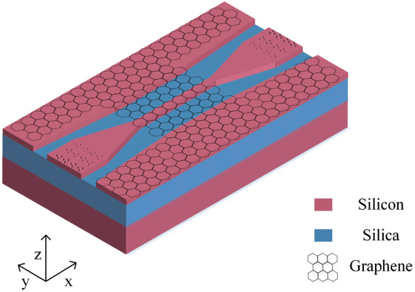
    Fig. 1. Schematic of GSHWs consisting of a graphene pad, a strip waveguide, and photonic crystal gratings.
    Surface dynamic conductivity of monolayer graphene versus its (a) chemical potential and (b) wavelength of incident light.
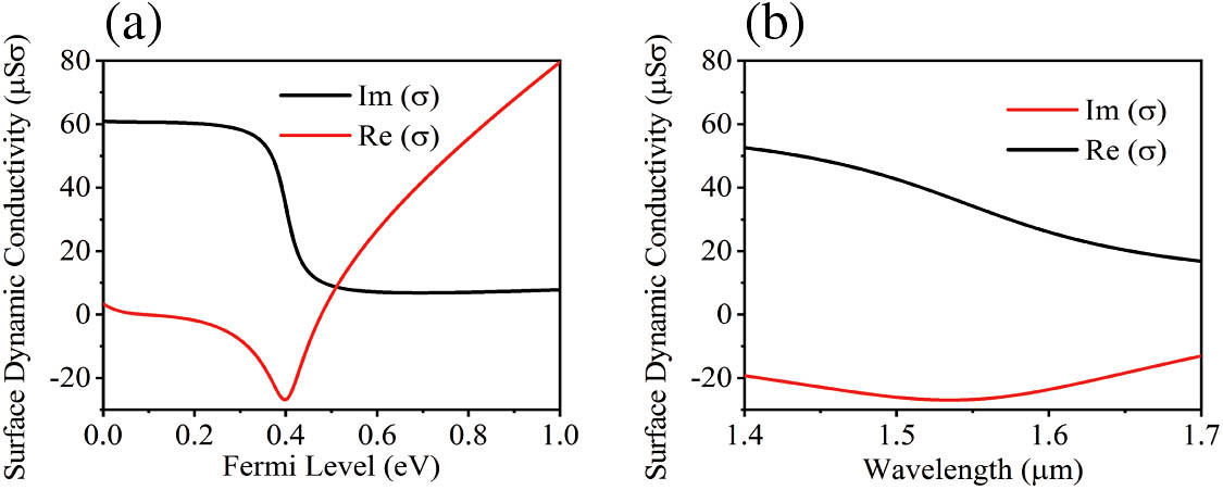
    Fig. 2. Surface dynamic conductivity of monolayer graphene versus its (a) chemical potential and (b) wavelength of incident light.
    (a)–(c) Real and imaginary parts of ERI and LAC at 500-nm width, 220-nm height, and 1550-nm wavelength with Fermi levels ranging from 0.12 eV to 0.6 eV for TE and TM modes, respectively. (d) The MDs are calculated with 10-μm-long graphene (the insets are electric field profiles of the TE mode at 1.4 and 1.7 μm wavelengths, respectively). (e) The MDs for TM mode under the same conditions.
    Fig. 3. (a)–(c) Real and imaginary parts of ERI and LAC at 500-nm width, 220-nm height, and 1550-nm wavelength with Fermi levels ranging from 0.12 eV to 0.6 eV for TE and TM modes, respectively. (d) The MDs are calculated with 10-μm-long graphene (the insets are electric field profiles of the TE mode at 1.4 and 1.7 μm wavelengths, respectively). (e) The MDs for TM mode under the same conditions.
    (a), (b) Simulated MDs depending on the width and height of GSHWs with the Fermi level of 0.4 eV and 10-μm-long graphene pad for the TE and TM modes, respectively. (c) The dependence of MDs on the different lengths of graphene for the TE and TM modes with the 500-nm-wide waveguide and Fermi level of 0.4 eV.
    Fig. 4. (a), (b) Simulated MDs depending on the width and height of GSHWs with the Fermi level of 0.4 eV and 10-μm-long graphene pad for the TE and TM modes, respectively. (c) The dependence of MDs on the different lengths of graphene for the TE and TM modes with the 500-nm-wide waveguide and Fermi level of 0.4 eV.
    (a) Raman spectra of the GSHWs (the inset figure is the SEM picture of graphene pad, the blue circle represents the spot where graphene is etched off, the red circle represents the spot where graphene is protected). (b) The experimental transmission data and fitted curves as a function of input power for the TE mode. Here, the relative transmission is expressed as T−ToTo×100%. (c) The comparison of MDs in simulated and experimental results with 10-, 15-, 20-, and 30-μm-long graphene pads (the GSHW with 30-μm-long graphene is not saturated sufficiently with the maximum power of the femtosecond laser we use. Here, we use the fitted MD of 30.1% from the measured data).
    Fig. 5. (a) Raman spectra of the GSHWs (the inset figure is the SEM picture of graphene pad, the blue circle represents the spot where graphene is etched off, the red circle represents the spot where graphene is protected). (b) The experimental transmission data and fitted curves as a function of input power for the TE mode. Here, the relative transmission is expressed as TToTo×100%. (c) The comparison of MDs in simulated and experimental results with 10-, 15-, 20-, and 30-μm-long graphene pads (the GSHW with 30-μm-long graphene is not saturated sufficiently with the maximum power of the femtosecond laser we use. Here, we use the fitted MD of 30.1% from the measured data).
    (a) Schematic of the experimental system. (b) Time history of the modulated probe light with the pump light acquired by the oscilloscope (OSC). (c) Time profile of a probe pulse (the inset is the temporal profile of a pump pulse).
    Fig. 6. (a) Schematic of the experimental system. (b) Time history of the modulated probe light with the pump light acquired by the oscilloscope (OSC). (c) Time profile of a probe pulse (the inset is the temporal profile of a pump pulse).
    Change in transmission of the probe light as a function of its time delay relative to the pump light. The FWHM is about 1.65 ps.
    Fig. 7. Change in transmission of the probe light as a function of its time delay relative to the pump light. The FWHM is about 1.65 ps.
    Hong Wang, Ningning Yang, Limin Chang, Chaobiao Zhou, Shiyu Li, Meng Deng, Zhenwei Li, Qiang Liu, Chi Zhang, Zhiyong Li, Yi Wang. CMOS-compatible all-optical modulator based on the saturable absorption of graphene[J]. Photonics Research, 2020, 8(4): 468
    Download Citation