• Photonics Research
  • Vol. 10, Issue 9, A106 (2022)
Yaocheng Shi1、*, Yong Zhang2, Yating Wan3、4, Yu Yu5, Yuguang Zhang6、7, Xiao Hu6、7, Xi Xiao6、7, Hongnan Xu1、8, Long Zhang1, and Bingcheng Pan1
Author Affiliations
  • 1Centre for Optical and Electromagnetic Research, State Key Laboratory for Modern Optical Instrumentation, College of Optical Science and Engineering, Zhejiang University, Zijingang Campus, Hangzhou 310058, China
  • 2State Key Laboratory of Advanced Optical Communication Systems and Networks, Department of Electronic Engineering, Shanghai Jiao Tong University, Shanghai 200240, China
  • 3Institute for Energy Efficiency, University of California Santa Barbara, Santa Barbara, California 93106, USA
  • 4Electrical and Computer Engineering Department, King Abdullah University of Science and Technology (KAUST), Thuwal 23955-6900, Saudi Arabia
  • 5Wuhan National Laboratory for Optoelectronics & School of Optical and Electronic Information, Huazhong University of Science and Technology, Wuhan 430074, China
  • 6National Information Optoelectronics Innovation Center, China Information and Communication Technologies Group Corporation (CICT), Wuhan 430074, China
  • 7State Key Laboratory of Optical Communication Technologies and Networks, China Information and Communication Technologies Group Corporation (CICT), Wuhan 430074, China
  • 8Department of Electronic Engineering, The Chinese University of Hong Kong, Shatin, New Territories, Hong Kong, China
  • show less
    DOI: 10.1364/PRJ.456772 Cite this Article Set citation alerts
    Yaocheng Shi, Yong Zhang, Yating Wan, Yu Yu, Yuguang Zhang, Xiao Hu, Xi Xiao, Hongnan Xu, Long Zhang, Bingcheng Pan. Silicon photonics for high-capacity data communications[J]. Photonics Research, 2022, 10(9): A106 Copy Citation Text show less
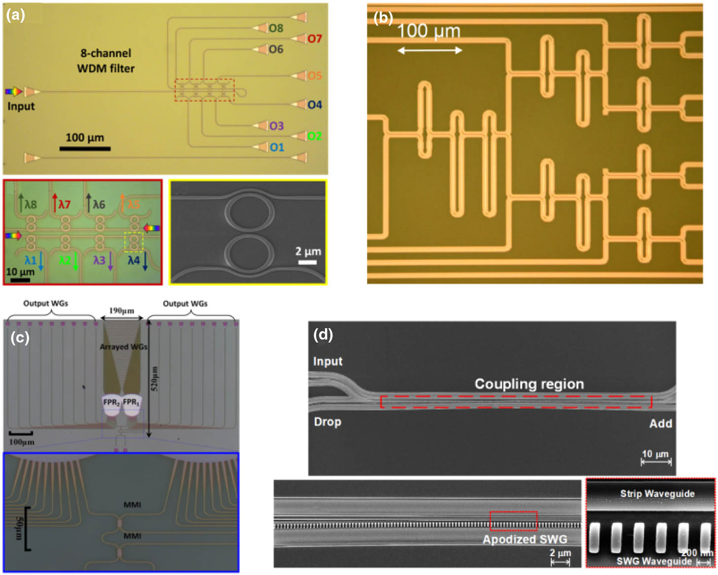
    (a) Optical microscope and scanning electron microscope (SEM) photos of an eight-channel add-drop filter based on second-adiabatic elliptical-MRRs [18]; (b) micrograph of a cascaded MZI (de)multiplexer [20]; (c) optical micrographs of a bidirectional AWG and an MZI-based interleaver [4]; (d) SEM photos of a contradirectional coupler based on an apodized SWG [21].
    Fig. 1. (a) Optical microscope and scanning electron microscope (SEM) photos of an eight-channel add-drop filter based on second-adiabatic elliptical-MRRs [18]; (b) micrograph of a cascaded MZI (de)multiplexer [20]; (c) optical micrographs of a bidirectional AWG and an MZI-based interleaver [4]; (d) SEM photos of a contradirectional coupler based on an apodized SWG [21].
    (a) SEM photos of a PBS based on grating-assisted contradirectional couplers [36]; (b) SEM photo of a cut-cornered polarization rotator [37]; (c) SEM photo of a PSR based on multimode waveguide and mode converter [38]; (d) micrographs of a PSR employing a nonlinearly tapered double-etched ADC structure [39].
    Fig. 2. (a) SEM photos of a PBS based on grating-assisted contradirectional couplers [36]; (b) SEM photo of a cut-cornered polarization rotator [37]; (c) SEM photo of a PSR based on multimode waveguide and mode converter [38]; (d) micrographs of a PSR employing a nonlinearly tapered double-etched ADC structure [39].
    (a) SEM photo of a three-mode multiplexer based on a shallow-etched MMI [75]; (b) illustration of mode multiplexer using asymmetric Y junctions [68]; (c) micrographs of a 10-channel mode multiplexer based on ADC structures [70]; (d) photos of a 16-channel mode (de)multiplexer (TE0−TE15) using gradient-duty-cycle SWGs [76].
    Fig. 3. (a) SEM photo of a three-mode multiplexer based on a shallow-etched MMI [75]; (b) illustration of mode multiplexer using asymmetric Y junctions [68]; (c) micrographs of a 10-channel mode multiplexer based on ADC structures [70]; (d) photos of a 16-channel mode (de)multiplexer (TE0TE15) using gradient-duty-cycle SWGs [76].
    Various configurations of carrier depletion PN junctions. (a) Lateral PN junction, (b) vertical PN junction, (c) L-shaped PN junction, (d) U-shaped PN junction, (e) interleaved PN junction, and (f) lateral PN junction with doping compensation.
    Fig. 4. Various configurations of carrier depletion PN junctions. (a) Lateral PN junction, (b) vertical PN junction, (c) L-shaped PN junction, (d) U-shaped PN junction, (e) interleaved PN junction, and (f) lateral PN junction with doping compensation.
    Schematic of silicon modulator. (a) MZM, (b) MRR modulator.
    Fig. 5. Schematic of silicon modulator. (a) MZM, (b) MRR modulator.
    (a) High-bandwidth MZM with substrate removed [135], (b) electronic–photonic synergistically designed silicon photonics transmitters [137], (c) lump-segmented silicon transmitter with six lumped phase shifters [138].
    Fig. 6. (a) High-bandwidth MZM with substrate removed [135], (b) electronic–photonic synergistically designed silicon photonics transmitters [137], (c) lump-segmented silicon transmitter with six lumped phase shifters [138].
    (a) High speed MRM for next generation energy-efficient optical networks beyond 100 Gbaud [147], (b) push-pull silicon dual-ring modulator with enhanced optical modulation amplitude [148], (c) 4×40 Gb/s O-band WDM silicon photonic transmitter based on MRMs [149].
    Fig. 7. (a) High speed MRM for next generation energy-efficient optical networks beyond 100 Gbaud [147], (b) push-pull silicon dual-ring modulator with enhanced optical modulation amplitude [148], (c) 4×40  Gb/s O-band WDM silicon photonic transmitter based on MRMs [149].
    Structure of the hybrid Si/LN MZM. (a) Schematic of the structure of the whole circuit; (b) schematic of the cross section of the hybrid waveguide; (c) SEM image of the cross section of the LN waveguide; (d) SEM image of the metal electrodes and the optical waveguide; (e) schematic of the VAC; (f) SEM images of the cross sections of the VAC at different positions (A, B, C) and calculated mode distributions associated with the cross sections.
    Fig. 8. Structure of the hybrid Si/LN MZM. (a) Schematic of the structure of the whole circuit; (b) schematic of the cross section of the hybrid waveguide; (c) SEM image of the cross section of the LN waveguide; (d) SEM image of the metal electrodes and the optical waveguide; (e) schematic of the VAC; (f) SEM images of the cross sections of the VAC at different positions (A, B, C) and calculated mode distributions associated with the cross sections.
    (a) Cross section (upper) and transverse field profile (lower) of a heterogeneous DFB laser design with an embedded spacer layer [194]. (b) Triple-ring mirror based tunable laser [195]: schematic illustration, SEM image of a Si/III–V taper, coarse tuning spectra showing the tuning range of 110 nm. (c) III–V/Si/SiN4 laser with SiN-based spiral [196]: schematic illustration, cross-section SEM image of the InP/Si gain, comparison of temperature-dependent wavelength shift of the III–V/Si/SiN laser and of a typical one with Si-based mirror.
    Fig. 9. (a) Cross section (upper) and transverse field profile (lower) of a heterogeneous DFB laser design with an embedded spacer layer [194]. (b) Triple-ring mirror based tunable laser [195]: schematic illustration, SEM image of a Si/III–V taper, coarse tuning spectra showing the tuning range of 110 nm. (c) IIIV/Si/SiN4 laser with SiN-based spiral [196]: schematic illustration, cross-section SEM image of the InP/Si gain, comparison of temperature-dependent wavelength shift of the III–V/Si/SiN laser and of a typical one with Si-based mirror.
    (a) Heterogeneous integration allows spectral coverage beyond the 1310 and 1550 nm telecom windows, with the shortest wavelength being 900 nm [198] and the longest wavelength being 4800 nm [199]. (b) Heterogeneous QD laser: schematic image (left) and simulated cross-sectional fundamental transverse-electric (TE) mode electrical field distributions (right). (c) Frequency noise spectrum of a heterogeneous QD laser showing that Lorentzian linewidth of 26 kHz is achieved [200].
    Fig. 10. (a) Heterogeneous integration allows spectral coverage beyond the 1310 and 1550 nm telecom windows, with the shortest wavelength being 900 nm [198] and the longest wavelength being 4800 nm [199]. (b) Heterogeneous QD laser: schematic image (left) and simulated cross-sectional fundamental transverse-electric (TE) mode electrical field distributions (right). (c) Frequency noise spectrum of a heterogeneous QD laser showing that Lorentzian linewidth of 26 kHz is achieved [200].
    (a) Normal-incidence structure; waveguide-integrated structures: (b) butt-coupling, (c) bottom-up coupling, (d) top-down coupling, (e) side-coupling (top view) schemes.
    Fig. 11. (a) Normal-incidence structure; waveguide-integrated structures: (b) butt-coupling, (c) bottom-up coupling, (d) top-down coupling, (e) side-coupling (top view) schemes.
    (a) Lateral homojunction, (b) lateral heterojunction, (c) vertical heterojunction PIN PDs.
    Fig. 12. (a) Lateral homojunction, (b) lateral heterojunction, (c) vertical heterojunction PIN PDs.
    100G CWDM-4 QFSP28 transceiver module of Intel.
    Fig. 13. 100G CWDM-4 QFSP28 transceiver module of Intel.
    400G DR4 transmitter with 4×100 Gb/s data paths of Intel.
    Fig. 14. 400G DR4 transmitter with 4×100  Gb/s data paths of Intel.
    Chip-on-board 800G silicon photonics transmitter.
    Fig. 15. Chip-on-board 800G silicon photonics transmitter.
    Integrated copackaged optical IO switch package with 16 photonic engines (PEs).
    Fig. 16. Integrated copackaged optical IO switch package with 16 photonic engines (PEs).
    Monolithic electronic-photonic systems based on a 65 nm transistor bulk CMOS process technology [296].
    Fig. 17. Monolithic electronic-photonic systems based on a 65 nm transistor bulk CMOS process technology [296].
    Schematic configurations for single-mode networks (first column), multimode networks (second column), and ring-bus networks (third column). (a), (b) The single-mode carriers can be arbitrarily routed by leveraging MRR or Mach–Zehnder switch (MZS) arrays. (c), (d) For multimode operations, the fabrics can be constructed by assembling mode MUXs and a single-mode NoC. (e), (f) The ring-bus NoCs support multiple carriers transferring in a single ring-like bus waveguide, which can be realized by utilizing WDM or MDM technologies. NoC, network on chip; MRR, micro-ring resonator; MZS, Mach–Zehnder switch; MUX, (de)multiplexer; WDM, wavelength-division multiplexing; MDM, mode-division multiplexing; WADM, wavelength add-drop (de)multiplexer; MADM, mode add-drop (de)multiplexer.
    Fig. 18. Schematic configurations for single-mode networks (first column), multimode networks (second column), and ring-bus networks (third column). (a), (b) The single-mode carriers can be arbitrarily routed by leveraging MRR or Mach–Zehnder switch (MZS) arrays. (c), (d) For multimode operations, the fabrics can be constructed by assembling mode MUXs and a single-mode NoC. (e), (f) The ring-bus NoCs support multiple carriers transferring in a single ring-like bus waveguide, which can be realized by utilizing WDM or MDM technologies. NoC, network on chip; MRR, micro-ring resonator; MZS, Mach–Zehnder switch; MUX, (de)multiplexer; WDM, wavelength-division multiplexing; MDM, mode-division multiplexing; WADM, wavelength add-drop (de)multiplexer; MADM, mode add-drop (de)multiplexer.
    (a) The single-mode NoC based on MRR array [299], under Creative Commons license CC BY. (b) The single-mode NoC based on MZS array [300], under Creative Commons license CC BY. NoC, network on chip; MRR, micro-ring resonator; MZS, Mach–Zehnder switch.
    Fig. 19. (a) The single-mode NoC based on MRR array [299], under Creative Commons license CC BY. (b) The single-mode NoC based on MZS array [300], under Creative Commons license CC BY. NoC, network on chip; MRR, micro-ring resonator; MZS, Mach–Zehnder switch.
    (a) The multimode NoC based on MRR array [338], under Creative Commons license CC BY. (b) The multimode NoC based on MZS array [339], under Creative Commons license CC BY. NoC, network on chip; MRR, micro-ring resonator; MZS, Mach–Zehnder switch.
    Fig. 20. (a) The multimode NoC based on MRR array [338], under Creative Commons license CC BY. (b) The multimode NoC based on MZS array [339], under Creative Commons license CC BY. NoC, network on chip; MRR, micro-ring resonator; MZS, Mach–Zehnder switch.
    (a) The ring-bus NoC based on WDM [345], under Creative Commons license CC BY. (b) The bus-ring NoC based on MDM [346], under Creative Commons license CC BY. NoC, network on chip; WDM, wavelength-division multiplexing; MDM, mode-division multiplexing.
    Fig. 21. (a) The ring-bus NoC based on WDM [345], under Creative Commons license CC BY. (b) The bus-ring NoC based on MDM [346], under Creative Commons license CC BY. NoC, network on chip; WDM, wavelength-division multiplexing; MDM, mode-division multiplexing.
    ReferenceTypeLoss (dB)ER (dB)BW (nm)FSR/Spacing (nm)Channels
    [11]Submicrometer MRR1.8>170.8932×2
    [16]Vernier racetrack/10.2/37.522×2
    [17]High-order MRR2500.0080.41×2
    [18]Elliptical MRR1.5451.43.21×8
    [20]Cascaded MZI1.615/2.41×8
    [22]Two-stage MZI0.413.6514.71×2
    [27]400 GHz AWG3.2917/3.21×12
    [28]400 GHz AWG2.3220.5/3.28×8
    [29]100 GHz AWG2.4517.1/0.84×4
    [30]25 GHz AWG/4/0.2512×512
    [31]MZI+AWG515/0.81×32
    [32]Asymmetric grating0.5810/33×3
    [33]Multimode grating0.5246>401×4
    Table 1. State-of-the-Art Wavelength Multiplexing Devicesa
    ReferenceTypeLoss (dB)XT (dB)BW (nm)
    [36]Grating-assisted contra directional couplers13020 (XT>30  dB)
    [38]Multimode waveguide0.5730.8285 (XT>20  dB)
    [34]Symmetrical DC<0.515C-band (XT>15  dB)
    [35]Asymmetric DC<130100 (XT>25  dB)
    [40]Cascaded bent DC<0.353570 (XT>30  dB)
    [41]Hetero-anisotropic metamaterials<1>20200 (XT>20  dB)
    [42]Pixelated DC1.5314.2253 (XT>14  dB)
    [46]Si3N4-assisted mode evolution13060 (XT>30  dB)
    [51]Mode-hybridization21740 (XT>17  dB)
    [58]ADC0.612C-band (XT>12  dB)
    [60]Bent DC<11870 (XT>18  dB)
    [61]Double-etched DC0.52030 (XT>20  dB)
    Table 2. State-of-the-Art Polarization Management Devices
    ReferenceTypeLoss (dB)XT (dB)BW (nm)Channels
    [65]MMIs<128C-band (XT>28  dB)3
    [68]Y junctions1.530C-band (XT>30  dB)2
    [70]ADCs1.81590 (XT>15  dB)10
    [71]Plasmonic waveguide0.3517100 (XT>17  dB)2
    [72]Inverse design waveguide82080 (XT>20  dB)3
    [73]MMIs and tapered phase shifter13760 (XT>37  dB)3
    [74]MMIs0.3624.460 (XT>20  dB)3
    [75]Shallow-etched MMI2.41070 (XT>10  dB)3
    [76]SWGs0.8–5.29.2–24/16
    [79]Asymmetric Y junction/34300 (XT>34  dB)2
    [82]Counter-tapered couplers<0.7410100 (XT>10  dB)2
    Table 3. State-of-the-Art Mode Multiplexing Devices
    ReferenceTypeLoss (dB)XT (dB)Channels
    [90]SiN-waveguide-assisted edge couplera<0.5236
    [93]Triple-tip inverse taper13.27.32
    [91]Mode-evolution counter-tapersa5.1254
    [92]SU8-waveguide-assisted edge coupler5/4
    [89]Subwavelength grating coupler6.1/4
    Table 4. State-of-the-Art Couplers for Few-Mode Fiber Coupling
    ReferenceTypeBW (GHz)Vπ·L  (V·cm)IL (dB)Length (mm)Data Rate (Gb/s)
    [103]MZM42.62.09/0.5140
    [131]MZM471.355.42.5225
    [136]MZM>501.45.42128
    [137]MZM/1.56.92.47100
    [167]MZM471.45.42.5305
    [166]IQ-MZM281.25.62500
    [112]MRM500.52/0.01b128
    [146]MRM>670.8/0.008b200
    [147]MRM770.53/0.006b192
    [154]Push-pull MRM42/14a0.015b144
    [168]MRM>670.8/0.008b302
    [169]PDM-MRM///0.005b256
    [145]PDM-MRM//10.01b260
    [161]PhC modulator38.6//0.01670
    Table 5. State-of-the-Art Silicon Modulators
    ReferenceTypeλ (μm)Vr (V)Id (nA)R (A/W)BW (GHz)
    [242]VPIN1.5511.61.040
    [244]VPIN1.53130.845
    [231]LPIN1.55140000.8120
    [262]LPIN1.5511001.070
    [243]LPIN1.55140.7467
    [263]LPIN1.5522000.3265
    1000.45240
    [233]VPIN1.55230000.7560
    [246]VPIN1.553610.8560
    [261]VPIN1.5536.40.8980
    [248]LPIN1.55281.16>50
    [254]LPIN1.55141.2317
    [253]LPIN1.5511001.27
    Table 6. State-of-the-Art Waveguide Si-Ge PIN Photodiodesa
    ReferenceTypeλ (μm)Vb (V)Rp (A/W)Id (nA)BW (GHz)GBP (GHz)BR (Gb/s)S at BER (dBm)
    [269]VSACM1.31250.551.2411.53401028 at 1012
    [267]MSM1.313.50.439.53001013.9 at 109
    [270]VSACM1.55230.81329.51030.4 at 1012
    [268]LPIN1.5570.420111901026 at 107
    [271]VSACM1.55100.750.44232762516 at 1012
    [272]VSACM1.31180.70.4262522.5 at 1012
    [273]VSACM1.5526.50.351304604013.9 at 1012
    [266]VSAM1.5560.48118.92842511.4 at 104
    [274]VSACM1.31120.212261505016 at 104
    [275]VPIN4.2401128 at 104
    [264]LSACM1.31120.6530273005018.6 at 104
    [5]LPIN1.5512.50.951033240649.2 at 106
    [276]VSACM1.3119.60.550.52818010616.8 at 104
    Table 7. State-of-the-Art Si–Ge APDs for High-Speed Optical Communicationsa
    Yaocheng Shi, Yong Zhang, Yating Wan, Yu Yu, Yuguang Zhang, Xiao Hu, Xi Xiao, Hongnan Xu, Long Zhang, Bingcheng Pan. Silicon photonics for high-capacity data communications[J]. Photonics Research, 2022, 10(9): A106
    Download Citation