Significance Owing to excellent adaptability to different working conditions, flexible electronics have attracted significant attention in many fields, such as wireless communication, human-machine interaction, and personal healthcare. Functional parts and conductive circuits are the basic components of electronics that respond to external stimulus and conduct signals, respectively.
Nanomaterials with unique physical and chemical properties are widely used for developing flexible electronics. Noble metals, such as silver, gold, and platinum are good candidates for manufacturing conductive parts because of their high conductivity and chemical stability. However, the high price of these metals limits their large scale production. Recently, copper has been considered a good alternative to noble metals for developing conductive component owing to its low-cost and excellent electrical properties. Furthermore, copper oxides (cuprous oxide and cupric oxide) are important transition metal oxides because of their semiconductive properties. They have been widely used as functional parts owing to their high sensitivity for external stimulation, such as humidity, temperature. Efficient manufacturing methods for materials play a major role in developing high-performance devices.
The typical “bottom-up” process, such as hydrothermal and chemical precipitation, provides a low-cost, precise control, and large-scale synthesis route to manufacture the micro/nanostructured copper. However, post-treatment processes, such as printing and sintering, are required to obtain the desired properties in a device. Such step-by-step manufacturing requires the cooperation of various techniques, which increases the process cost and complexity. Thus, developing a low-cost process for manufacturing the micro/nanostructures has attracted significant attention.
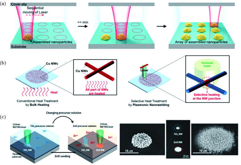
Direct laser writing, as an advanced processing technology developed recently, provides a novel approach for micro/nanostructure manufacturing. This technology has been used to process the structure, including noble metals, metal oxides, and carbon-based materials. In this study, the technical characteristics of manufacturing copper-based micro/nanostructures with direct laser writing have been summarized.
Progress The typical laser processing of micro/nanostructures, such as laser assembly, sintering, and synthesis, has been elaborated (
Conclusions and Prospect In summary, direct laser writing has been an efficient manufacturing process for copper micro/nanostructures owing to its noncontact, maskless, and rapid processing characteristics. Direct laser writing based on ionic precursors integrates the synthesis, positioning, assembly, and joining of copper nanomaterials into a one-step, which shows unique advantages in structure and composition control. This process still faces challenges in processing copper structures, such as the accurate control of products, diversification of composite structures, and further expansion of application. Further, in-depth study is needed to explore the writing mechanism and fully understand the processing characteristics for copper-based micro/nanostructures.