
Yuying Hu, Chen Qiu, Tao Shen, Kaike Yang, Huixiong Deng. Direct calculations on the band offsets of large-lattice-mismatched and heterovalent Si and III–V semiconductors[J]. Journal of Semiconductors, 2021, 42(11): 112102
- Journal of Semiconductors
- Vol. 42, Issue 11, 112102 (2021)
Abstract
1. Introduction
As the size of transistors continues to shrink, there is an urgent need to replace traditional electrical interconnects with Si-based optical interconnects that have the advantages of fast transmission speed, high bandwidth, and multiplexability to boost computer performances[
However, unlike isovalent superlattices and alloys[
Over the years, some models have been proposed and try to overcome the above problems, mainly by adding deformation potential to remove the influence of strain on energy levels. For example, Van de Walle et al.[
In this paper, we present a modified, and reliable method for calculating the band offset of large lattice mismatch and heterovalent semiconductors, and simultaneously apply this to the calculations of band offsets of Si/III–V systems. We found that our proposed approach has the same accuracy as the widely used modified core level method for systems with small lattice mismatch. Moreover, the calculated results are much closer to the experimental values of the large-lattice-mismatched and heterovalent systems.
2. The method of band offset calculation
The calculations were performed using density functional theory[
The valence band offset is usually calculated as follows[
Here
(i) Bulk semiconductors of AX and BY. This step is to perform separate bulk calculations for two semiconductors AX and BY at their equilibrium lattice constant. The different
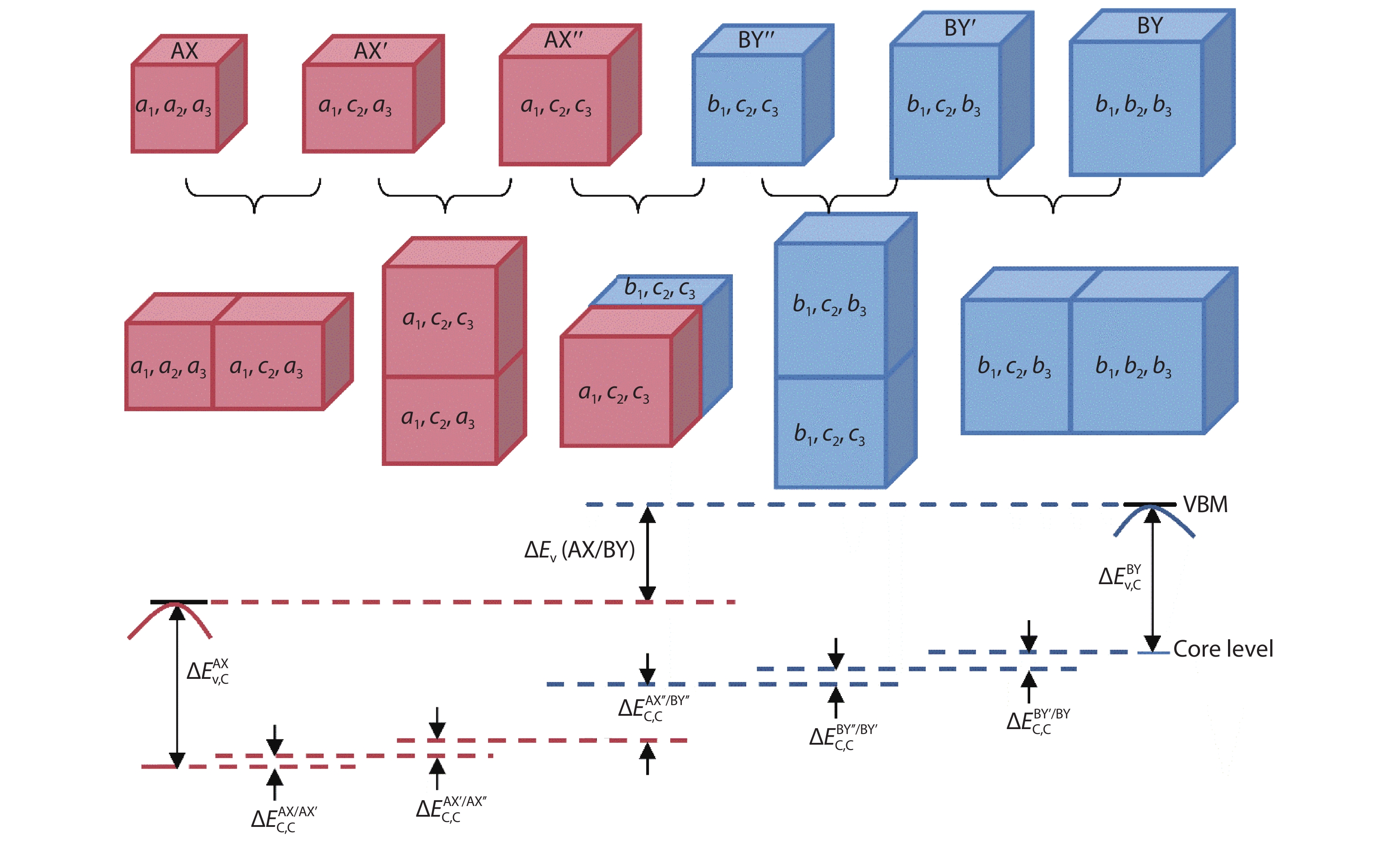
(ii) Alignment of core energy levels in heterojunctions. The purpose of this step is to align the core energy levels in isolated systems of AX and BY, and which is achieved through a five-step calculation, as proposed by the Lang et al.[
![]()
Figure 1.(Color online) Five steps for correcting the effect of lattice mismatch on valence band offset calculations using core energy levels as a reference.
where
(iii) Reconstructed polarized interface. The purpose of this step is to reconstruct the interface to eliminate the internal electric field caused by the heterovalence in the polarized interface structures. When Si and III–V semiconductors form the heterojunction along the direction of [100] or [111], because they do not belong to the same group and the valence electrons are different, there is often a built-in electric field in the system[
![]()
Figure 2.(Color online) (a–e) show the five superlattice structures constructed. (a) Equilibrium-unidirectional superlattice of Si. (b) Unidirectional-bidirectional strain superlattice of Si. (c) Bidirectional strain superlattice of Si and InAs. (d) Bidirectional-unidirectional superlattice of InAs. (e) Unidirectional-equilibrium superlattice of InAs.
3. Applications to large-lattice-mismatched and heterovalent Si and III–V semiconductors
The valence band offsets of Si and III–V semiconductors with zincblende structure along [100], [110], and [111] directions have been calculated, respectively. We choose the Si/InAs superlattice as an example, which has a lattice mismatch of 11.60%.Fig. 2 shows the five constructed superlattice structures of Si and InAs along the [100] direction. They are the equilibrium-unidirectional strain superlattice of Si, the unidirectional-bidirectional strain superlattice of Si, the bidirectional strain superlattice of Si and InAs, the bidirectional-unidirectional strain superlattice of InAs, and the unidirectional strain-equilibrium superlattice of InAs, respectively.
Fig. 3 shows the elimination of the interface potential between Si and InAs. The abrupt interface refers to the interface directly connected by Si and InAs, and the mixed anion interface refers to the structure in which anions are mixed in the interface, and the mixed cation interface is the same. Fig. 3 clearly shows that the electrostatic potential at the abrupt interface is oblique, indicating the presence of a built-in electric field. When the interface atoms are mixed, the electrostatic potential becomes flat, indicating that the built-in electric field is eliminated successfully.
![]()
Figure 3.(Color online) The abrupt interface, mixed cation interface and mixed anion interface formed by Si and InAs along the [100] direction, and the corresponding potential distribution along the growth orientation of the superlattices.
The calculated valence band offsets are shown in Table 1. First of all for the system with small lattice mismatch, we compared with previous theoretical calculations without considering strain and built-in electric field as well as with the experimental measurement and found almost no difference. For example, for Si/AlP systems with a lattice mismatch of 0.55%, the valence band offset in the [100] direction is calculated to be –0.88 eV in this paper, in agreement with the previous theoretical value of –0.91 eV[
For systems with a large lattice mismatch, the results obtained by our method are in good agreement with the experimental measurements. For example, for the Si/GaN system with lattice mismatch up to –16.57%, our calculated values are –1.95, –2.00, and –1.60 eV for the [100], [110], [111] directions, respectively, which are close to the experimental value of –1.90 eV[
Combining the valence band offset with the experimentally measured band gap[
![]()
Figure 4.(Color online) Band offset diagram of the Si/GaSb, Si/InAs and Si/InSb systems with zinc-blende structure along the [100], [110], and [111] directions. The energy is relative to the vacuum level of Si.
4. Conclusions
We present a modified method for theoretically calculating the band offset of large-lattice-mismatched and heterovalent semiconductors for the different directions based on the first-principles calculations. Using this method, the effect of interface reconstruction and lattice mismatch on band offsets is corrected by considering the reconstruction of the heterovalent interface and the inclusion of unidirectional strain crystals that play a transitional role between the equilibrium crystal structure and the bidirectional strain structure. Furthermore, we apply the method to calculate the band offsets of heterovalent Si and III–V semiconductors with large lattice mismatches in the [100], [110] and [111] directions. This research will provide some guidance for the selection of suitable light-source materials on the Si substrate from the perspective of energy band structure, and will be beneficial for the understanding and analysis of the properties of heterojunctions between the Si substrate and zincblende structured III–V semiconductors.
Acknowledgments
This work was supported by the National Key Research and Development Program of China (Grant No. 2018YFB2200100), the Key Research Program of the Chinese Academy of Sciences (Grant No. XDPB22), and the National Natural Science Foundation of China (Grant No. 118764347, 11614003, 11804333). H. X. D. was also supported by the Youth Innovation Promotion Association of Chinese Academy of Sciences (Grant No. 2017154).
References
[1] Y A Bioud, A Boucherif, M Myronov et al. Uprooting defects to enable high-performance III–V optoelectronic devices on silicon. Nat Commun, 10, 4322(2019).
[2] M Zacharias, P C Kelires. Temperature dependence of the optical properties of silicon nanocrystals. Phys Rev B, 101, 245122(2020).
[3] P Lu, D Li, Y Cao et al. Si nanocrystals-based multilayers for luminescent and photovoltaic device applications. J Semicond, 39, 061007(2018).
[4] S Zhao, X Liu, X Pi et al. Light-emitting diodes based on colloidal silicon quantum dots. J Semicond, 39, 061008(2018).
[5] J Zheng, Z Liu, C Xue et al. Recent progress in GeSn growth and GeSn-based photonic devices. J Semicond, 39, 061006(2018).
[6] G Boras, X Yu, H Liu. III–V ternary nanowires on Si substrates: growth, characterization and device applications. J Semicond, 40, 101301(2019).
[7] J Zhang, X Yang, Y Feng et al. Vacancy-engineering-induced dislocation inclination in III-nitrides on Si substrates. Phys Rev Mater, 4, 073402(2020).
[8] C Zhao, B Xu, Z Wang et al. Boron-doped III–V semiconductors for Si-based optoelectronic devices. J Semicond, 41, 011301(2020).
[9] S Chen, W Li, J Wu et al. Electrically pumped continuous-wave III–V quantum dot lasers on silicon. Nat Photonics, 10, 307(2016).
[10] C Shang, A C Gossard, J E Bowers et al. Low-threshold epitaxially grown 1.3-μm InAs quantum dot lasers on patterned (001) Si. IEEE J Sel Top Quantum Electron, 25, 1502207(2019).
[11] C G Van de Walle. Band lineups and deformation potentials in the model-solid theory. Phys Rev B, 39, 1871(1989).
[12] H X Deng, J W Luo, S H Wei. Chemical trends of stability and band alignment of lattice-matched II–VI/III–V semiconductor interfaces. Phys Rev B, 91, 075315(2015).
[13] T Mano, H Fujioka, K Ono et al. InAs nanocrystal growth on Si (100). Appl Surf Sci, 130, 760(1998).
[14] R Heitz, N N Ledentsov, D Bimberg et al. Optical properties of InAs quantum dots in a Si matrix. Appl Phys Lett, 74, 1701(1999).
[15] J Tersoff. Theory of semiconductor heterojunctions: The role of quantum dipoles. Phys Rev B, 30, 4874(1984).
[16] C Bru-Chevallier, A El Akra, D Pelloux-Gervais et al. InGaAs quantum dots grown by molecular beam epitaxy for light emission on Si substrates. J Nanosci Nanotechnol, 11, 9153(2011).
[17] Y H Li, A Walsh, S Chen et al. Revised ab initio natural band offsets of all group IV, II–VI, and III–V semiconductors. Appl Phys Lett, 94, 212109(2009).
[18] L Lang, Y Y Zhang, P Xu et al. Three-step approach for computing band offsets and its application to inorganic ABX3 halide perovskites. Phys Rev B, 92, 075102(2015).
[19] P Hohenberg, W Kohn. Inhomogeneous electron gas. Phys Rev, 136, B864(1964).
[20] W Kohn, L J Sham. Self-consistent equations including exchange and correlation effects. Phys Rev, 140, A1133(1965).
[21] D M Ceperley, B J Alder. Ground state of the electron Gas by a stochastic method. Phys Rev Lett, 45, 566(1980).
[22] G Kresse, J Furthmüller. Efficiency of ab-initio total energy calculations for metals and semiconductors using a plane-wave basis set. Phys Rev Lett, 6, 15(1996).
[23]
[24] S H Wei, A Zunger. Calculated natural band offsets of all II–VI and III–V semiconductors: Chemical trends and the role of cation d orbitals. Appl Phys Lett, 72, 2011(1998).
[25] H X Deng, B Huang, S H Wei. Stable interface structures of heterovalent semiconductor superlattices: The case of (GaSb)
[26] N E Christensen. Dipole effects and band offsets at semiconductor interfaces. Phys Rev B, 37, 4528(1988).
[27] R Saive, H Emmer, C T Chen et al. Study of the interface in a GaP/Si heterojunction solar cell. IEEE J Photovolt, 8, 1568(2018).
[28] C B Han, C He, X J Li. Near-infrared light emission from a GaN/Si nanoheterostructure array. Adv Mater, 23, 4811(2011).
[29] R S List, J C Woicik, I Lindau et al. The Si/GaAs (110) heterojunction: Strain, disorder, and valence-band discontinuity. J Vac Sci Technol B, 5, 1279(1987).
[30] C G Van de Walle, R M Martin. Theoretical calculations of heterojunction discontinuities in the Si/Ge system. Phys Rev B, 34, 5621(1986).
[31] W Pollard. Valence-band discontinuities at semiconductor heterojunctions. J Appl Phys, 69, 3154(1991).
[32] N N Halder, P Biswas, B Nagabhushan et al. Effect of band offset on carrier transport and infrared detection in InP quantum dots/Si nano-heterojunction grown by metalorganic chemical vapor deposition technique. J Appl Phys, 115, 203719(2014).
[33] A D Katnani, G Margaritondo. Microscopic study of semiconductor heterojunctions: Photoemission measurement of the valance-band discontinuity and of the potential barriers. Phys Rev B, 28, 1944(1983).


Set citation alerts for the article
Please enter your email address

© Copyright 2018-2021 | Chinese Laser Press. All Rights Reserved 沪ICP备15018463号-20