Guocui Wang, Bin Hu, Yan Zhang. Dynamic Metasurface Design and Functional Devices[J]. Laser & Optoelectronics Progress, 2021, 58(9): 0900001
Search by keywords or author
- Laser & Optoelectronics Progress
- Vol. 58, Issue 9, 0900001 (2021)
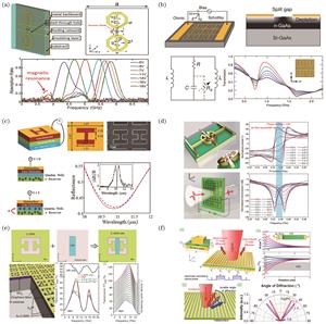
![Designs of electrically controlled metasurfaces based on different electrically sensitive materials. (a) Varactors are integrated into metaatoms[35]; (b) Schottky diode structure is formed by fabricating metaatom arrays on gallium arsenide substrate[39]; (c) semiconductor quantum well structure is inserted into bottom of metaatom arrays[41]; (d) two-dimensional electron gas is integrated into gap of metaatoms[42]; (e) graphene is inserted into gap of metaatoms[50]; (f) ITO transparent conductive film is embedded in bottom of metaatom arrays[51]](/richHtml/lop/2021/58/9/0900001/img_1.jpg)
Fig. 1. Designs of electrically controlled metasurfaces based on different electrically sensitive materials. (a) Varactors are integrated into metaatoms[35]; (b) Schottky diode structure is formed by fabricating metaatom arrays on gallium arsenide substrate[39]; (c) semiconductor quantum well structure is inserted into bottom of metaatom arrays[41]; (d) two-dimensional electron gas is integrated into gap of metaatoms[42]; (e) graphene is inserted into gap of metaatoms[50]; (f) ITO transparent conductive film is embedded in bottom of metaatom arrays[51]
![Designs of optically controlled metasurfaces based on semiconductor. (a) Semiconductor is used as substrate[52]; (b) semiconductor is filled in gap of metaatom[55]](/richHtml/lop/2021/58/9/0900001/img_2.jpg)
Fig. 2. Designs of optically controlled metasurfaces based on semiconductor. (a) Semiconductor is used as substrate[52]; (b) semiconductor is filled in gap of metaatom[55]
Fig. 3. Designs of metasurfaces controlled by temperature based on different thermal sensitive materials. (a) Vanadium dioxide film is inserted into bottom of metaatom arrays[61]; (b) vanadium dioxide film is integrated into gap of metaatom[62]; (c) rod-shaped metaatom is fabricated with vanadium dioxide materials[63]; (d) C-shaped metaatom is fabricated with vanadium dioxide materials[64]
Fig. 4. Designs of mechanically controlled metasurfaces. (a) Metaatoms are fabricated on stretchable substrate[76]; (b) part of metaatoms is fabricated on deformable cantilever[70]; (c) microfluidic channel is integrated into metaatom arrays[74]; (d) double layer metasurfaces with relative space movement[81]
Fig. 5. Designs of magnetically controlled metasurface or chemically doped dynamic metasurface. (a) Magnetically controlled active metasurfaces by embedding magnetic material Ce1Y2Fe5O12 (Ce∶YIG) into metasurfaces[87]; (b) chemically controlled programable metasurfaces based on metal-dielectric phase transition of rod shaped metaatom made from magnesium (Mg) in hydrogen environment[89]
Fig. 6. Spectrum modulation devices based on uniformly controlled dynamic metasurfaces. (a) Optially controlled terahertz tunable filter[54]; (b) electrically controlled tunable filter[92]; (c) multi-wavelength terahertz modulator based on optical control[95]; (d) multi-wavelength terahertz perfect tunable absorber based on optical control[99]
Fig. 7. Polarization control devices based on uniformly controlled dynamic metasurfaces. (a) Polarization conversion device with large angle incidence based on microfluidic technology[78]; (b) metasurface polarization converter device consists of cantilever bendable metaatoms[102]
Fig. 8. Light field modulation by dynamic metasurfaces based on uniform control. (a) Electrically controlled microwave aberration-free metalens[106]; (b) temperature-controlled visible light zoom metalens[110]; (c) light-controlled fast polarization converter and dynamic beam splitter[117]; (d) mechanically controlled dynamic controller for beam deflection angle[118]; (e) mechanically controlled two-color tunable metasurfaces hologram[120]; (f) chemically controlled special beam converter[89]
Fig. 9. Designs of dynamic reconfigurable/programable metasurfaces by individually controlling metaatoms. (a) Biased diode is integrated in metaatoms, and metaatoms are individually controlled by field-programmable gate array[122]; (b) predesigned metaatom arrays with different order of arrangement are loaded into pump laser by DMD, and the corresponding pattern is transferred on silicon wafer to reconfigure metasurface devices with different functions when silicon wafer is pumped by laser[123]
Fig. 10. Applications of dynamic configurable/programable metasurface. (a) Encode electromagnetic waves by optically driven digital metasurface to achieve stealth of external targets, radar detection, and special beam generation and dynamic switching[128]; (b) different binary phase information is encoded on metasurface, realizing real-time dynamic imaging of different patterns[131]; (c) programmable coded metasurface is used for directly transmitting digital signals in optical communications[134]
|
Table 1. Spectrum modulation parameters based on dynamic metasurface

Set citation alerts for the article
Please enter your email address


