1Shanghai Jiao Tong University, Department of Electronic Engineering, State Key Laboratory of Advanced Optical Communication Systems and Networks, Shanghai, China
2Nokia Bell Labs, Murray Hill, New Jersey, United States
3Shanghai University, Key Laboratory of Specialty Fiber Optics and Optical Access Networks, Joint International Research Laboratory of Specialty Fiber Optics and Advanced Communication, Shanghai, China
4Shanghai Jiao Tong University, School of Electronic Information and Electrical Engineering, John Hopcroft Center for Computer Science, Shanghai, China
Mode-division multiplexing (MDM) technology enables high-bandwidth data transmission using orthogonal waveguide modes to construct parallel data streams. However, few demonstrations have been realized for generating and supporting high-order modes, mainly due to the intrinsic large material group-velocity dispersion (GVD), which make it challenging to selectively couple different-order spatial modes. We show the feasibility of on-chip GVD engineering by introducing a gradient-index metamaterial structure, which enables a robust and fully scalable MDM process. We demonstrate a record-high-order MDM device that supports TE0–TE15 modes simultaneously. 40-GBaud 16-ary quadrature amplitude modulation signals encoded on 16 mode channels contribute to a 2.162 Tbit / s net data rate, which is the highest data rate ever reported for an on-chip single-wavelength transmission. Our method can effectively expand the number of channels provided by MDM technology and promote the emerging research fields with great demand for parallelism, such as high-capacity optical interconnects, high-dimensional quantum communications, and large-scale neural networks.
To manage the explosive growth of data streams, optical interconnect has emerged as a promising solution with the merits of large bandwidth, low transmission losses, and inherent parallelism enabled by various physical dimensions of the optical carrier.1 Mode, as an important degree of freedom, can be leveraged to construct parallel data streams to accommodate a projected 30-fold data traffic growth2 for the optical interconnect systems3 and provide scalability for a wide range of on-chip applications, such as nonlinear optics4 and optical sensing.5 It also contributes to emerging fields of research where parallelism is in great demand, such as quantum communications6,7 and AI computing.8 For instance, high-dimensional Hilbert spaces can be encoded in terms of waveguide modes, leading to high-capacity and noise-robust quantum communications.9 For large-scale neural networks, it is desired to process operations in parallel by mapping the weight and vector elements onto different modes for hardware accelerating.8 These applications indicate the great potential of multimode operation in future high-capacity optical networks and novel integrated photonic circuits.
In the past decade, researchers have conducted extensive studies on integrated multimode photonics, such as mode-division multiplexing (MDM),3,10–15 mode switching,16 multimode bending,17–21 and crossing.22–24 High data rate MDM transmissions were also demonstrated by employing spatial modes to carry high-speed optical signals.21,25,26 MDM is among the most important techniques for multimode photonics, capable of generating and multiplexing orthogonal spatial modes. Most reported on-chip mode multiplexers (MUXs) are based on phase-matching approaches,3,27 by designing structural parameters to match the propagation constants of waveguide modes for efficient mode coupling. However, the phase-matching condition is determined by the group-velocity dispersion (GVD),4 which varies significantly between waveguide modes, thus imposing challenges to achieve an efficient mode coupling and limiting the scaling of MDM technology toward high-order modes and more parallel spatial channels. In photonic waveguides, the GVD can be manipulated either by engineering the waveguide confinement or using new materials.4 Most of the previous MDM works were based on waveguide dimension engineering approaches.28 More specifically, adiabatic tapers are employed to relax the stringent phase-matching conditions for MDM, at the cost of large footprints, which impose challenges for high-density integration.14 The introduction of new materials may be of great interest, which provides a new degree of freedom for engineering GVD between waveguide modes by transmitting signals in different materials, thus enabling robust mode couplings and the high-order MDM. However, limited by the available material choices29 and the feasibility of the fabrication process,30 most of the reported MDM works are based on single material platforms, where GVD largely limits the achievable MDM order.
Enabled by the increasingly high resolution of advanced lithography, metamaterial has emerged as a new candidate for designing silicon-on-insulator (SOI)-based devices.31 Researchers have demonstrated the use of all-dielectric metamaterials for optical cloaking,32 neuromorphic computing,33 and transformation optics applications.34,35 In these works, silicon metamaterials construct various artificial effective medium devices with tailorable refractive indices and dispersion properties, which make them possible to guide light in a desired manner without introducing materials other than silicon. Thus, it is feasible to manipulate the GVD for waveguide modes using metamaterial engineering, offering unprecedented flexibilities for multimode device design. In previous works, metamaterial structures were employed to introduce dielectric perturbations and tune the mode overlap within a multimode waveguide, which enable arbitrary mode conversions36–38 and multimode routings.39 However, most reported metamaterial-based MDM devices operate exclusively in the conventional phase-matching regime, where the GVD between waveguide modes still exists, thus limiting the achievable MDM orders and channel count. To the best of our knowledge, the maximum number of reported MDM channels is eight prior to our recent work, where cascaded asymmetrical directional couplers are utilized to (de)multiplex signals on different modes.38 In our previous work, subwavelength grating (SWG), as one of the simplest metamaterial architectures,40–42 has been introduced to engineer the GVD between modes and relax the stringent phase-matching conditions, thus enabling an 11-channel MDM.43 However, the performance of the device is largely determined by the fabrication accuracies, and the channel counts are challenging to be further scaled, limited by the available duty cycle choices defined by the lithography resolutions.
Sign up for Advanced Photonics TOC. Get the latest issue of Advanced Photonics delivered right to you!Sign up now
In this paper, we demonstrate a robust and fully scalable mode coupling method by leveraging the gradient index metamaterial (GIM) structure. Different from previous phase-matching approaches, the coupling strength in the proposed scheme can be effectively tailored by engineering the parameters of the GIM waveguides. This scheme has been proposed to achieve an inter-layer coupling between the active InP layer and the passive optical layer.44 Adiabatic coupling enabled by the GIM coupler can help to relax the stringent phase matching condition encountered by conventional DCs and provides a new degree of freedom for designing an efficient mode coupling process and achieving a record 16-channel (–) on-chip MDM device.45 Here, we conduct a detailed theoretical analysis, provide a full characterization of the device, and carry out a high-speed data transmission experiment. The measured transmission capacity reaches , which is the highest data rate ever reported for an on-chip single-wavelength transmission. The record MDM channel count and the total data rate demonstrated in this paper highlight the large potential of MDM technology for the arising fields of research, such as high-capacity optical interconnects, high-dimensional quantum communications, large-scale neural networks, and full characterization sensing applications.
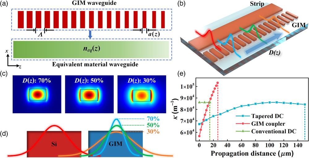
Figure 1(a) shows the conceptional illustration of the GIM waveguide. Silicon nanorods are arranged on a predefined pattern with the duty cycle varying along the propagation direction ( axis). With the adoption of the subwavelength-scale nanostructure, it is feasible to tailor the refractive index distribution as well as the anisotropy properties by engineering the structural parameters. This provides large design flexibilities for controlling the fundamental attributes of electromagnetic waves, such as amplitude, phase, polarization, and wavefront. Here, we focus on the coupling between a GIM waveguide and a nanowire waveguide, as shown in Fig. 1(b). The GIM waveguide is designed with a linearly decreasing duty cycle along the propagation direction, which corresponds to a linearly decreasing refractive index distribution . We calculate the equivalent material refractive index of the subwavelength-scale structure using effective-medium theory42 (detailed information can be found in Sec. 1 in the Supplementary Material). Figure 1(c) shows the simulated electric field distributions of GIM waveguides with different duty cycles using a finite-difference eigenmode (FDE) solver. It can be noted that the GIM waveguide with a larger duty cycle exhibits a much stronger electric field confinement at the waveguide center, which can be attributed to the larger refractive index contrast between the effective-medium core and the cladding. This property makes it feasible to manipulate the electric field and the refractive index distributions for planar waveguide devices by varying the duty cycle of the GIM waveguide, as shown in Fig. 1(d), which enables a new degree of freedom for on-chip coupling strength engineering.
Figure 1.Planar-metamaterial-enabled refractive-index-distribution manipulation and GIM-enabled adiabatic coupling. (a) Conceptional illustration of a 1D metamaterial structure with a linearly decreasing duty cycle , which can be regarded as a strip waveguide with a varying refractive index . (b) Schematic configuration of a GIM-based mode coupling process. The GIM waveguide is tailored with a linear duty cycle distribution along the propagation direction. (c) Simulated electric field distributions of GIM waveguides with different duty cycles. (d) Cross-section view of the GIM-based direction coupler. The Gaussian curves illustrate the power distributions of the modes supported by the GIM waveguide. (e) Calculated coupling coefficients for the tapered DC, GIM coupler, and conventional DC as functions of the propagation distance.
We characterize the coupling strength of the GIM coupler by calculating the coupling coefficient using coupled mode theory.46 The coupled mode equations can be written as where and are the amplitudes of the supported waveguide modes and , respectively. and are the propagation constants, and and are the coupling coefficients. Since the refractive index and the electric field distributions of the GIM-based coupler are all -dependent, we calculate and at selected evenly distributed positions: where and are the electric field distributions of the waveguide modes and , respectively. is the cross section of the GIM-based coupler, and is the refractive index contrast between the cladding () and the equivalent material of the GIM waveguide. To illustrate the benefits of introducing the GIM structure, we calculate the coupling coefficients as functions of the propagation distance for the single mode GIM coupler, conventional DC, and tapered DC, respectively. The dashed lines in Fig. 1(e) mark the coupling lengths we choose to enable a full power transfer from a 400-nm-wide nanowire waveguide to (i) a waveguide tapered from 250 to 550 nm; (ii) a GIM waveguide with its duty cycle varying from 30% to 70%; and (iii) a 400-nm strip waveguide, respectively. The gaps for the three architectures are chosen as 200 nm. Figure 1(e) shows the calculated coupling coefficients. The conventional DC exhibits the most compact footprint but is sensitive to fabrication deviations. The GIM coupler outperforms the other two types of DCs with much larger coupling coefficients, mainly due to the low optical field confinement of the GIM structure, which results in a compact footprint. In addition, the coupling coefficient tuning range of the GIM coupler is significantly larger than that of the taper structure, which enables large flexibilities to manipulate by engineering the distribution.
By taking advantage of the adiabatic coupling and fabrication tolerant properties of the GIM coupler, we show its applications in high-order mode generation and multi-channel MDM. Figure 2(a) shows the schematic configuration of the GIM coupler-based mode (de)multiplexing design for selective mode coupling. The duty cycle of the GIM waveguide linearly increases from 30% to 70% while maintaining a fixed period value . The feature size of the device is calculated as , which is feasible to be fabricated using E-beam lithography. We choose the width of the GIM waveguide as and the gap between two waveguides as . The bus waveguides that support high-order modes are designed to operate under weak-confinement conditions, where the effective refractive indices are chosen as to ensure a sufficient mode overlap at the coupling region without introducing excess losses. The widths of the silicon bus waveguides for different spatial modes are calculated using an FDE solver. Here, we take the mode as an example to illustrate the high-order mode excitation process. Since the two waveguides are placed closely, evanescent fields can interact with each other according to the coupled mode theory. We calculate the coupling coefficients between the Bloch mode in the GIM waveguide and all the supported eigen-modes in the bus waveguide for a GIM coupler with a bus waveguide width of . It can be noted that the coupling coefficient linearly increases along the propagation direction with the incorporation of the GIM structure, as shown in Fig. 2(b), which facilitates the power transfer from the mode in the bus waveguide to the Bloch mode in the GIM waveguide. The coupling between other waveguide modes to the Bloch modes is suppressed due to the negligible coupling coefficients, which can be attributed to the well-confined mode profiles. We optimize the structural parameters of the GIM-based coupler for selective mode coupling separately using the 3D-finite difference time domain method (ANSYS Lumerical). The coupling length is to meet the adiabatic criteria, and we use SWG-based waveguide bends to gradually separate the coupling region with a bending radius of . Here, we consider the mode demultiplexing process by injecting a high-order mode from the bus waveguide and monitoring the output from the GIM waveguide. Figure 2(c) shows the simulated electric field distribution for the mode demultiplexing process. The injected mode is adiabatically coupled to the fundamental Bloch mode in the GIM waveguide. Further information of the simulations and optimizations of the field distributions and the optimized structural parameters for other waveguide modes can be found in Sec. 3 in the Supplementary Material. To verify the feasibility of the GIM coupler to achieve a robust high-order mode coupling, we simulate the mode demultiplexing process using the GIM structure, the conventional DC, and the tapered DC, respectively, as shown in Fig. 2(d). It can be noted that the conventional DC is very sensitive to fabrication deviations; even a 1% dimension variation leads to significant performance degradations. The GIM coupler exhibits comparable tolerance performance to the tapered DC when the waveguide dimensions vary by . However, when the waveguide deviation is , the GIM coupler shows some performance advances, which can be attributed to its larger refractive index tuning range. These results show the feasibility for achieving a very-high-order MDM by employing the GIM structure. These results show the feasibility for achieving a very-high-order MDM by employing the GIM structure.
Figure 2.GIM-based coupler for 16-channel MDM. (a) Schematic configuration of the GIM-based coupler designed for selective mode coupling. The duty cycle of the GIM waveguide linearly increases from 30% to 70% along the propagation direction for constructing a linear refractive index distribution. (b) Calculated coupling coefficients and and the normalized transmission responses for the mode in the strip waveguide (mode ) and the Bloch mode in the GIM waveguide (mode ), as a function of propagation distance. (c) Simulated electric field distribution for the mode demultiplexing. (d) Simulated mode demultiplexing process using GIM structure, conventional DC, and tapered DC, respectively, when the waveguide dimension varies.
To verify the feasibility of the MDM technique in scaling the transmission capacity of optical waveguides, we cascade the GIM couplers designed for different spatial modes and construct a 16-channel MDM device, as shown in Figs. 3(a)–3(c). GIM waveguides are placed along a strip bus waveguide with a varying width to (de)multiplex selected waveguide modes, as shown in Fig. 3(a). We use adiabatic tapers to connect bus waveguides with different widths. Transition tapers with a length are used to convert the injected modes in the silicon nanowire waveguide to the Bloch modes in the GIM waveguides. The devices were fabricated on an SOI platform with a 220-nm-thick silicon on top of a buried oxide. Waveguides and the metamaterial structures were patterned using electron beam lithography (Vistec EBPG-) and fully etched by an inductively coupled plasma (ICP; SPTS) etching process. A -thick cladding layer was then deposited on top of the devices by plasma-enhanced chemical vapor deposition (PECVD, Oxford). Figure 3(b) shows the microscope image of the fabricated MDM device. A 34-channel fiber array is used to vertically couple the light between the optical fiber and the fabricated chip. Due to the lack of the waveguide cross-section imaging setup, we have not collected the output mode profiles of the multimode waveguide for mode purity analysis. Instead, a demultiplexer (deMUX) stage is cascaded at the end of the multimode waveguide to convert the orthogonal high-order modes back to fundamental modes for power monitoring. Figures 3(c)–3(f) provide the scanning electron microscope (SEM) images for the coupling regions of the GIM-based mode MUXs for selected mode channels.
Figure 3.GIM-based couplers for 16-channel MDM. (a) Schematic configuration of the 16-channel mode MUX. (b) Microscope image and (c) SEM image of the 16-channel GIM-based mode MUX and deMUX. (d)–(f) Magnified SEM images of the coupling regions.
To characterize the optical performance of the device, we use a continuous-wave tunable laser source (Keysight 81960A) to generate laser output ranging from 1507 to 1600 nm. A customized 34-channel fiber array is used to couple the light between fibers and the 16 input ports (–) and 16 output ports (–) of the device. We fix the input port and record the power output from all 16 output ports using an optical power meter (Keysight N7744A). A micro-electro-mechanical system (MEMS) optical switch is used to switch between channels. The wavelength sweep program runs repeatedly so the data are recorded for all 16 output ports when the MEMS switches between channels. Measured transmission results of the fabricated 16-channel mode deMUX are provided in Fig. 4. Light is injected from one input port to excite a corresponding high-order mode in the bus waveguide. Optical signals output from all 16 output ports are recorded as the transmission and crosstalk for the selected mode channels. The transmission spectra of the mode deMUX are normalized to that of the identical grating couplers fabricated on the same chip with a coupling loss. Measured insertion losses range from 0.96 to 6.95 dB, and the crosstalk values vary between and for all 16 channels at 1550 nm. Note that the mode experiences the largest insertion loss of 6.95 dB while exhibiting an acceptable crosstalk of . This performance degradation can be attributed to the relatively low fiber-to-chip coupling efficiency for this channel, caused by the defects observed at the corresponding grating coupler, which can be optimized through multiple iterations.
Figure 4.(a)–(p) Measured transmission responses of the 16-channel mode deMUX. Each subplot shows the transmission and crosstalk recorded at 16 output ports for a selected input channel.
To verify the feasibility of the proposed mode MUX for supporting parallel mode channels, we perform a high-speed data transmission experiment. The experimental setup is shown in Fig. 5(a). At the transmitter side, an external cavity laser (ECL) operated at 1550.12 nm with a 15 kHz linewidth is utilized as the light source. A 100-GSa/s dual-channel digital-to-analog converter (DAC) (MICRAM DAC10002) with a 3-dB bandwidth of 44 GHz is employed to generate a 40-GBaud Nyquist 16-ary quadrature amplitude modulation (16-QAM) signal with a roll-off factor of 0.01. After being amplified by two electrical amplifiers (SHF S807 C), the electrical 16-QAM signal drives a 22-GHz in-phase and quadrature modulator (Fujitsu FTM7961EX), which is biased at its transmission null. The generated optical 16-QAM signal is amplified and then time gated via an acousto-optic modulator with a duty cycle of 11.8% and a frequency of 12.5 kHz. To avoid transient power boost induced by signal gating, an amplified spontaneous emission (ASE) source is spectrally shaped by a wave shaper and combined with the time-gated signal via a polarization-maintaining coupler to emulate eight wavelength-division multiplexing (WDM) channels with a 50-GHz spacing. The generated WDM signals are boosted by two erbium-doped fiber amplifiers and then split into 16 copies as the inputs to the 16-channel MDM chip. To guarantee the correct characterization of the device, the 16 input data channels generated by an ECL laser are first decorrelated before entering the silicon chip by 15 fiber delay lines ranging from 1 to 15 km to ensure the data are decorrelated properly with a relative delay of 25 ns. The photographs of the testing platform are presented in the insets of Fig. 5(a), showing input and output polarization controller arrays and the vertical coupling platform (See Sec. 4 in the Supplementary Material for details).
Figure 5.High-speed data transmission experiment. (a) Experimental setup for the high-speed transmission experiment of the 16-channel MDM chip. The insets show the photographs of the testing platform and the fiber array-based vertical coupling. (b) Monitored optical spectrum of the recombined signal at the receiver side. (c) Calculated BERs of 40-GBaud 16-QAM signals for 16 modes after MIMO-FFE and MLSD. All channels are below the 15% FEC threshold. (d) Recovered constellations for all the 16 modes.
At the receiver side, the 16 channels are first polarization-division multiplexed (PDM) using 8 polarization beam combiners and then recombined chronologically to 8 time slots, which make it feasible to detect all the 16-channel signals via 1 polarization-diversity coherent receiver. The optical spectrum of the recombined signal is shown in Fig. 5(b). A tunable optical bandpass filter (EXFO XTM-50) with an edge slope of is used to select the signals located at the channel under test and filter out the ASE noise simultaneously. The local oscillator is gated and delayed in a similar manner. Finally, the detected electrical signals are captured by an digital storage oscilloscope (LeCroy 36Zi-A) with a 3-dB bandwidth of 36 GHz and processed offline via MATLAB. We employ multiple-input multiple-output (MIMO)-based digital signal processing (DSP) to tackle the mode mixing and recover the transmitted information streams. Detailed information about the MIMO-based DSP that was adopted can be found in Sec. 5 in the Supplementary Material. Figure 5(c) shows the calculated bit error ratios (BERs) of 40-GBaud 16-QAM signals for 16 modes after the MIMO-FFE and maximum likelihood sequence detection (MLSD) algorithm. The BERs for all 16 channels are below the 15% forward error correction (FEC) threshold. Considering the frame redundancy and 15% FEC overhead, we achieve the highest on-chip net data rate of [40 GBaud × 4 bits per symbol × 16 modes × 97.1% / (1 + 15%)] at a single wavelength by employing 16 parallel mode channels. Figure 5(d) shows the constellations of all 16 modes, which indicate that all 16 channels have good signal quality. A potential net spectral efficiency of [] can be obtained by further combining the WDM technology with 50 GHz channel spacing. While it is possible to recover signals using MIMO DSP as long as the transmission matrix is unitary47 when crosstalk performance is limited, researchers are also working on the crosstalk mitigation approach to enable an MIMO-free multi-channel transmission. We may further optimize the mode deMUX design to suppress undesired mode coupling to achieve a WDM-compatible MDM device.
5 Conclusion
We have proposed a high-order mode coupling process by introducing metamaterial structures. It is feasible to mitigate the GVD between waveguide modes by employing GIM waveguides for coupling strength engineering, which contributes to a robust and fully scalable MDM. We have demonstrated a record-high-order MDM supporting – mode channels and performed a high-speed data transmission experiment. A net data rate of has been achieved at a single wavelength. This high-order MDM approach is fully compatible with conventional WDM and PDM technologies. The effective MDM channel scaling may boost the arising fields of research where parallelism is in great demand, such as high-capacity optical interconnects, high-dimensional quantum communications, large-scale neural networks for hardware accelerating, and full characterization sensing.
Yu He received his BS degree from Nankai University, Tianjin, China, in 2015, and his PhD from Shanghai Jiao Tong University, Shanghai, China, in 2020. He is currently a postdoctoral fellow at Shanghai Jiao Tong University. His current research interests include integrated photonic devices, heterogeneous integrations, and metamaterials. He has published more than 60 journal and conference papers, including Light: Science & Application, Advanced Photonics, Journal of Lightwave Technology, and OFC/ ECOC/CLEO conferences, etc., with more than 1000 citations.
Yikai Su received his PhD in EE from Northwestern University, Evanston, Illinois, United States, in 2001. He worked at Crawford Hill Laboratory of Bell Laboratories, and joined Shanghai Jiao Tong University, Shanghai, China, as a full professor in 2004. His research areas cover silicon photonic devices, optical transmission, and signal processing. He has over 600 publications and gave >70 invited talks at conferences including OFC, CLEO, and IPS. He is a senior member of IEEE and a fellow of Optica.
Biographies of the other authors are not available.
[26] G. Chen et al. Silicon-photonics based remote-radio-head using mode and wavelength division multiplexing with capacity of 4.781 Tbit/s for radio-over-fiber massive MIMO, 1-3(2019).