
Bowen Bai, Fenghe Yang, Zhiping Zhou. Demonstration of an on-chip TE-pass polarizer using a silicon hybrid plasmonic grating[J]. Photonics Research, 2019, 7(3): 289
- Photonics Research
- Vol. 7, Issue 3, 289 (2019)
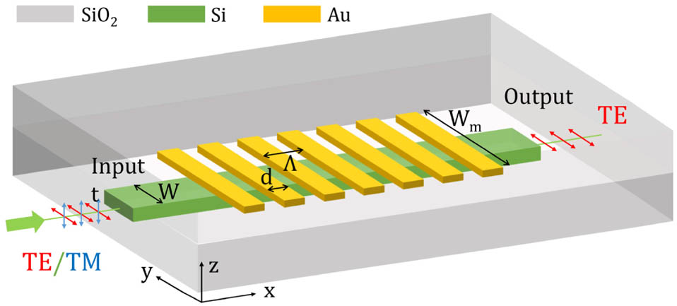
Fig. 1. 3D schematic of the proposed TE-pass polarizer on an SOI platform.
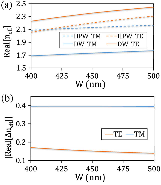
Fig. 2. (a) Real part of n eff Δ n eff W g = 50 nm
Fig. 3. (a) Mode similarity (between the hybrid plasmonic mode in the HPW and the photonic mode in the DW) and (b) the absolute value of the real part Δ n eff g W
Fig. 4. (a) ER and (b) IL as a function of metal strip length d N = 8 W = 450 nm g = 50 nm
Fig. 5. Optical energy flux density along the propagation direction from the top view when the TM or TE mode is injected. Here, W = 450 nm N = 8 d = 400 nm Λ = 750 nm
Fig. 6. SEM image of the fabricated TE-pass polarizer.
Fig. 7. (a) Normalized measured spectrum of one polarizer. (b) Corresponding ER and IL of the device. The black lines are trend lines extracted with robust locally weighted regression.
|
Table 1. Summary of Demonstrated TE-Pass Polarizers

Set citation alerts for the article
Please enter your email address
© Copyright 2018-2021 | Chinese Laser Press. All Rights Reserved 沪ICP备15018463号-20