Abstract
An on-chip, high extinction ratio transverse electric (TE)-pass polarizer using a silicon hybrid plasmonic grating is proposed and experimentally demonstrated. Utilizing plasmonics to manipulate the effective index and mode distribution, the transverse magnetic mode is reflected and absorbed, while the TE mode passes through with relatively low propagation loss. For a 6-μm-long device, the measurement result shows that the extinction ratio in the wavelength range of 1.52 to 1.58 μm varies from 24 to 33.7 dB and the insertion loss is 2.8–4.9 dB. Moreover, the structure exhibits large alignment tolerance and is compatible with silicon-on-insulator fabrication technology.1. INTRODUCTION
Silicon-on-insulator (SOI) is a prevailing and attractive platform for photonic integration. The feature of high index contrast between the silicon waveguide and cladding ( or air) enables devices in submicrometer dimensions; however, strong polarization dependence emerges simultaneously. The different propagation properties of transverse electric (TE) and transverse magnetic (TM) modes in such waveguides will degrade the performance of the photonic integrated chip. One solution is using polarization-independent devices [1,2]. Another is to use polarization diversity schemes [3] in which polarization splitting [4–6] and rotating [7–9] are applied. On-chip polarizers, serving as the third approach, can extinguish the unwanted polarization state in a system. Over the years, various configurations of polarizers with reasonable performance have been reported, as shown in Table 1. In principle, a polarizer should support only one polarization state while being lossy or cut off for the others. Traditional dielectric polarizers [10–15] usually have large footprints because of the relative low birefringence. For example, a polarizer utilizing shallowly etched SOI ridge waveguides [11] is proposed and the extinction ratio (ER) is 25 dB over a 100 nm wavelength range with 1 mm in length. Subwavelength grating (SWG) index engineering [13] is applied to satisfy the TM mode cut-off condition. The ER is 30 dB and the length of the structure is as long as 60 μm. To further shrink the device, Xu and Shi [15] demonstrated a TE-pass polarizer 29.4 μm in length by using an asymmetrical directional coupler. As the demand for dense photonic integration increases rapidly, new strategies to minimize the device size are eagerly needed.
| Reference No. | Device Length (μm) | ER (dB) | IL (dB) |
| [12] | 9 | 27 | 0.5 |
| [13] | 60 | 35 | 0.4 |
| [15] | 29.4 | 29.8 | 1.04 |
| [19] | 3 | 16.5 | 2.2 |
| [22] | 30 | 31 | 0.04 |
| [25] | 30 | 26 | 2.4 |
| [30] | 3.1 | 18 | 0.76 |
| This work | 6 | 37.8 | 4.6 |
Table 1. Summary of Demonstrated TE-Pass Polarizers
Recently, surface plasmon polaritons (SPPs) have been intensively investigated for polarization manipulation due to nanoscale optical field confinement [16] and natural polarization sensitivity. Various types of plasmonics-based polarizers have been reported, such as using a metal–insulator–metal (MIM) structure [17–19], a directional coupler (DC) [20–23], or a hybrid plasmonic waveguide (HPW) [24–26]. Compact polarizers utilizing the mode cutoff condition in the plasmonic slot region [17,18] have been proposed. The ERs are relatively low and the structures are difficult to fabricate using planar integrated technology. Huang et al. [19] fabricated a TE-pass polarizer using a narrow MIM waveguide. The insertion loss (IL) is 2.2 dB with an ER around 16 dB. For earlier HPW-based designs, the device length is relatively long (e.g., 17 μm [24] and 30 μm [25]) and the IL is relatively high [26]. To lower the IL, Sun et al. [22] demonstrated a DC-type plasmonic polarizer with an IL of 0.04 dB. The device is a bit long (30 μm) and an ER over 28 dB is achieved. Vertical coupling structures [14,23] were proposed theoretically. The ERs are not very high and the schemes require a complex double layer fabrication process, which is not compatible with conventional planar integrated techniques. Although hybrid plasmonic grating (HPG)-based polarizers have been proposed [27,28] and demonstrated [29,30], the fabrication process requires precise alignment between two lithography layers. In some structures, the width of the metal strip should be the same as the waveguide below [24,26]. Such stiff conditions further increase fabrication complexity.
In this paper, we experimentally demonstrate a TE-pass polarizer by using an HPG on an SOI platform. Because of the optical confinement of plasmonics, both the effective index and mode distribution can be manipulated. The TM mode is reflected and absorbed by the 6-μm-long HPG section, while the TE mode goes through with relatively low loss. Within the wavelength range of 1.52 to 1.58 μm, the measured ER varies from 24 to 33.7 dB and the IL is 2.8–4.9 dB. Different from other HPG-based polarizers, the demonstrated structure shows a large alignment tolerance and is compatible with SOI fabrication technology.
Sign up for Photonics Research TOC. Get the latest issue of Photonics Research delivered right to you!Sign up now
2. STRUCTURE AND PRINCIPLE
The proposed device (Fig. 1) is fabricated on a 220-nm-thick Si SOI platform with up-cladding. The width of the standard single-mode Si waveguides is . The HPG is the polarizer section, which consists of a silicon waveguide, a thin insertion layer with thickness of , and a certain number of metal strips with width of and height of . The period number is and the metal strip length is . Here, Au is chosen as the metal material.
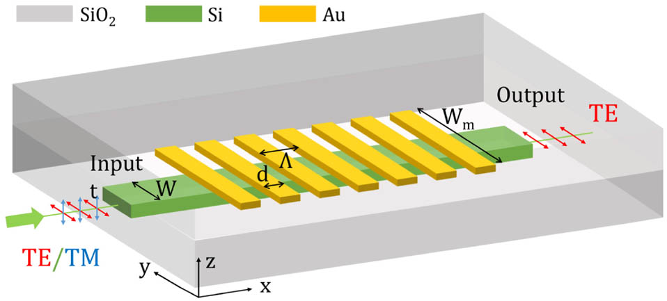
Figure 1.3D schematic of the proposed TE-pass polarizer on an SOI platform.
To achieve a TE-pass polarizer, the TM mode should be reflected or absorbed as much as possible by the HPG, while the TE mode should propagate through without distraction. The amount of reflection per unit length, defined as the coupling coefficient [31], can be written as in a traditional Bragg grating. Here, , , and are the mode effective index, mode effective indices difference (), and grating period, respectively. To avoid significant reflection for the TE mode, should be as small as possible, which is the opposite for the TM mode. The parameters of the structure should be carefully chosen to enhance the birefringence.
The 2D and 3D finite element methods (FEMs) are used to design the polarizer and study its characteristics. The operation wavelength is 1.55 μm, and the corresponding refractive indices for Au, , and Si are [32], 1.444, and 3.478, respectively. We calculate the real part of in DW and HPW. Real goes up as the waveguide width increases [Fig. 2(a)] because of the better optical confinement of the wider waveguide. The optical field confinement of plasmonics has different impacts on for different polarization states. The TE mode in a dielectric waveguide (DW) is a pure photonic mode, and most of the optical field is confined in the Si waveguide. However, the TE mode in an HPW contains a fraction of the SPP mode. Because the reflective index of Au is much smaller than that of Si, the for the TE mode in an HPW is a bit smaller than that in a DW. In contrast, the major optical field of the TM mode in a DW is distributed in the low-index cladding. Although the TM in an HPW is also a hybrid mode, the major optical field is tightly confined in the Si core, which results in a higher in the HPW. When is 450 nm, for the TE mode is 0.15, but is about 0.4 for the TM mode [Fig. 2(b)]. When the TE/TM modes launch from the input port, the TM mode will be quickly reflected by the HPG in several periods. for the TE mode slightly drops, while it remains almost unchanged for the TM mode as rises. Therefore, fabrication variations of the waveguide width have little impact on the performance of the polarizer.

Figure 2.(a) Real part of and (b) absolute value of the real part in the HPW and DW for TM and TE polarizations as a function of waveguide width . Here, the gap between the metal strip and the Si waveguide below is .
The thickness of insertion layer also significantly influences the mode reflection, particularly for the TM mode because of the large mode distribution mismatch. However, effective index analysis is insufficient and mode distribution should be taken into consideration for the design. We introduce the mode overlap ratio (, defined in Ref. [27]) to evaluate the mode distribution similarity of two polarizations in the HPW and DW [Fig. 3(a)] quantitatively. gets lower as decreases for both polarizations, indicating the rise of mode reflection. Mode distribution has a greater impact on the TM mode because . The low leads to significant scattering and reflection loss for the TM mode. The plasmonics-induced increase and large mode mismatch for the TM mode are conducive to reducing the device size. If choosing a smaller (e.g., ), the reflection for the TM mode will increase, and the device length can be very short. However, the propagation loss for the TE mode also rises significantly with a thin insertion layer, which agrees well with mode effective index analysis [Fig. 3(b)]. Here, we choose as a trade-off.
Figure 3.(a) Mode similarity (between the hybrid plasmonic mode in the HPW and the photonic mode in the DW) and (b) the absolute value of the real part in the HPW and DW for TM and TE polarizations as a function of insertion layer thickness . Here, waveguide width is 450 nm.
ER and IL are two key figures of merit for a polarizer, and are defined as where and are the normalized output power for the TE mode and the TM mode, respectively. For a good design, the ER should be large while the IL should be as small as possible. In our design, the number of periods is set to 8 in order to achieve a high ER over 20 dB when metal length varies from 380 to 440 nm. If we reduce the to 7 or less, ER will dramatically decrease. The grating period and the metal strip length also significantly influence ER and IL. ER increases as rises and reaches its maximum value of 28.6 dB with when and [Fig. 4(a)]. On the other hand, the IL is always a basic concern for plasmonic devices. With a fixed , IL decreases as rises, which means the reflection and mode distribution mismatch rather than metal absorption are the major losses for TE mode. Noticing that IL increases monotonically with increased grating period [Fig. 4(b)] as well, here we choose and as a compromise.
Figure 4.(a) ER and (b) IL as a function of metal strip length with period variation from 730 to 760 nm. Here, , , and .
Further simulation has been carried out to confirm the principle (Fig. 5). It can be seen that the TE mode passes through the HPG, while the TM mode disappears gradually due to the reflection, mode distribution mismatch, and metal absorption. At 1550 nm, the ER achieves 26.9 dB with an IL of 3.4 dB in the above case. Although the reflective index difference and mode distribution mismatch between the DW and the HPW for the TM mode can be further increased by decreasing the insertion layer thickness, which results in a shorter length of the polarizer, the IL will dramatically rise at the same time.
Figure 5.Optical energy flux density along the propagation direction from the top view when the TM or TE mode is injected. Here, , , , and .
The designed TE-pass polarizer was fabricated on a standard SOI wafer with 220-nm-thick top silicon and 2-μm-thick buried dioxide. First, a 1.6-μm-thick electron beam resist, PMMA, was spun on the SOI substrate and electron-beam lithography (EBL) was used to define the waveguide pattern. Then a coupled plasma etching process followed to fully etch the silicon waveguide. A 220-nm-thick layer is deposited by the magnetron sputtering method while retaining the e-beam resist. After removing the PMMA resist, a 50-nm-thick layer was deposited using plasma-enhanced chemical vapor deposition (PECVD). To locate the metal layer, 340-nm-thick ZEP 520 resist was used and followed by EBL. Then, 5 nm Ti (adhesion layer) and 100 nm Au were deposited using thermal evaporation, and a lift-off process was introduced to form the HPG section. Finally, the chip was covered with a 2-μm-thick silica layer as the upper cladding by PECVD. Figure 6 shows the top-view scanning electron microscope (SEM) picture of the fabricated polarizer, captured before the upper silica cladding was deposited.
Figure 6.SEM image of the fabricated TE-pass polarizer.
To characterize the fabricated polarizer, a tunable CW laser with a 1.52–1.58 μm wavelength range is used as the light source. A digital polarization controller is used to control the polarization state. Light is coupled into the sample through tapered lens fiber and then coupled out to an optical spectrum analyzer (OSA) to get the spectrum of the output. A series of HPG-based polarizers with different periods and duty cycles were fabricated. The reference waveguides are exactly the same as the polarizers except that they have no metal strips. With a fixed period, the metal length varies from 380 to 430 nm.
The measured transmission spectrum [Fig. 7(a)] and the corresponding ER and IL [Fig. 7(b)] of one polarizer are shown in Fig. 7. The fluctuations in the curves are mainly from fabrication-introduced surface roughness and defects of the metal strips. The output power of the TE mode is much higher than that of the TM mode. Since the performance of the OSA responds better when the output power is higher, the curve of the TE mode is relatively flat, while that of the TM mode fluctuates. The signal-to-noise ratio is also degraded by the reflections of both end facets and the external disturbances. To efficiently estimate the noise, a robust locally weighted regression method [33] is used to extract the trend lines. The fitting parameter used here is 0.25. To guarantee measurement accuracy, each device is tested three times, and the mean values are considered as the final results. The measured ER within the wavelength range of 1.52 to 1.58 μm varies from 24 to 33.7 dB and the IL is 2.8–4.9 dB. At 1.55 μm, the IL is 4.6 dB, which is about 1.2 dB higher than the theoretical calculation. In the practical fabrication process, a 5-nm-thick Ti layer was used as an adhesion layer. The optical loss of Ti is higher than that of Au, which contributes to a fraction of the absorption loss. The thickness of the low-index insertion layer may be less than 50 nm due to fabrication error, which leads to a higher ER with a bit larger IL. The surface roughness of metal and waveguide may cause extra scattering loss. The IL can be further reduced by optimizing fabrication and choosing better materials, such as optimizing the metal deposition and lift-off process, choosing better adhesion materials or other metal (e.g., Cu that does not need an adhesion layer), using the thermal oxidation method instead of PECVD to form the thin spacer layer and increasing its thickness to reduce scattering and reflection, and optimizing the lithography and etching processes for smaller sidewall roughness.
Figure 7.(a) Normalized measured spectrum of one polarizer. (b) Corresponding ER and IL of the device. The black lines are trend lines extracted with robust locally weighted regression.
3. CONCLUSION
We have proposed and experimentally demonstrated an on-chip TE-pass polarizer based on an HPG. Not only the effective index but also mode overlap is taken into consideration for the design. Utilizing the unique strong optical field confinement property of plasmonics to manipulate the effective index and mode distribution, the TM mode is reflected and absorbed by the plasmonic grating, while the TE mode passes through with relatively low loss. Within the wavelength range of 1.52 to 1.58 μm, the measured ER of the 6-μm-long device is 24 to 33.7 dB, and the corresponding IL is 2.8 to 4.9 dB. This device is compatible with SOI fabrication technology and can be easily integrated with other optical components. Moreover, the structure exhibits large alignment tolerance and paves the way to realize flexible on-chip polarization manipulation.
References
[1] Q. Deng, Q. Yan, L. Liu, X. Li, J. Michel, Z. Zhou. Robust polarization-insensitive strip-slot waveguide mode converter based on symmetric multimode interference. Opt. Express, 24, 7347-7355(2016).
[2] L. Liu, Q. Deng, Z. Zhou. Subwavelength-grating-assisted broadband polarization-independent directional coupler. Opt. Lett., 41, 1648-1651(2016).
[3] T. Barwicz, M. R. Watts, M. A. Popović, P. T. Rakich, L. Socci, F. X. Kärtner, E. P. Ippen, H. I. Smith. Polarization-transparent microphotonic devices in the strong confinement limit. Nat. Photonics, 1, 57-60(2007).
[4] B. Bai, Q. Deng, Z. Zhou. Plasmonic-assisted polarization beam splitter based on bent directional coupling. IEEE Photon. Technol. Lett., 29, 599-602(2017).
[5] L. Gao, F. Hu, X. Wang, L. Tang, Z. Zhou. Ultracompact and silicon-on-insulator-compatible polarization splitter based on asymmetric plasmonic-dielectric coupling. Appl. Phys. B, 113, 199-203(2013).
[6] L. Liu, Q. Deng, Z. Zhou. Manipulation of beat length and wavelength dependence of a polarization beam splitter using a subwavelength grating. Opt. Lett., 41, 5126-5129(2016).
[7] L. Gao, Y. Huo, J. S. Harris, Z. Zhou. Ultra-compact and low-loss polarization rotator based on asymmetric hybrid plasmonic waveguide. IEEE Photon. Technol. Lett., 25, 2081-2084(2013).
[8] L. Gao, Y. Huo, K. Zang, S. Paik, Y. Chen, J. S. Harris, Z. Zhou. On-chip plasmonic waveguide optical waveplate. Sci. Rep., 5, 15794(2015).
[9] B. Bai, L. Liu, Z. Zhou. Ultracompact, high extinction ratio polarization beam splitter-rotator based on hybrid plasmonic-dielectric directional coupling. Opt. Lett., 42, 4752-4755(2017).
[10] S. I. H. Azzam, M. F. O. Hameed, N. F. F. Areed, M. M. Abd-Elrazzak, H. A. El-Mikaty, S. S. A. Obayya. Proposal of an ultracompact CMOS-compatible TE-/TM-pass polarizer based on SOI platform. IEEE Photon. Technol. Lett., 26, 1633-1636(2014).
[11] D. Dai, Z. Wang, N. Julian, J. E. Bowers. Compact broadband polarizer based on shallowly-etched silicon-on-insulator ridge optical waveguides. Opt. Express, 18, 27404-27415(2010).
[12] X. Guan, P. Chen, S. Chen, P. Xu, Y. Shi, D. Dai. Low-loss ultracompact transverse-magnetic-pass polarizer with a silicon subwavelength grating waveguide. Opt. Lett., 39, 4514-4517(2014).
[13] Y. Xiong, D. X. Xu, J. H. Schmid, P. Cheben, W. N. Ye. High extinction ratio and broadband silicon TE-pass polarizer using subwavelength grating index engineering. IEEE Photon. J., 7, 7802107(2015).
[14] S. I. Azzam, S. S. A. Obayya. Ultra-compact resonant tunneling-based TE-pass and TM-pass polarizers for SOI platform. Opt. Lett., 40, 1061-1064(2015).
[15] H. Xu, Y. Shi. On-chip silicon TE-pass polarizer based on asymmetrical directional couplers. IEEE Photon. Technol. Lett., 29, 861-864(2017).
[16] D. K. Gramotnev, S. I. Bozhevolnyi. Plasmonics beyond the diffraction limit. Nat. Photonics, 4, 83-91(2010).
[17] Z. Ying, G. Wang, X. Zhang, Y. Huang, H. Ho, Y. Zhang. Ultracompact TE-pass polarizer based on a hybrid plasmonic waveguide. IEEE Photon. Technol. Lett., 27, 201-204(2015).
[18] T. K. Ng, M. Z. M. Khan, A. Al-Jabr, B. S. Ooi. Analysis of CMOS compatible Cu-based TM-pass optical polarizer. IEEE Photon. Technol. Lett., 24, 724-726(2012).
[19] Y. Huang, S. Zhu, H. Zhang, T. Liow, G. Lo. CMOS compatible horizontal nanoplasmonic slot waveguides TE-pass polarizer on silicon-on-insulator platform. Opt. Express, 21, 12790-12796(2013).
[20] B. Ni, J. Xiao. Plasmonic-assisted TE-pass polarizer for silicon-based slot waveguides. IEEE Photon. Technol. Lett., 30, 463-466(2018).
[21] B. Ni, J. Xiao. A compact silicon-based TE-pass polarizer using three-guide directional couplers. IEEE Photon. Technol. Lett., 29, 1631-1634(2017).
[22] X. Sun, M. Mojahedi, J. S. Aitchison. Hybrid plasmonic waveguide-based ultra-low insertion loss transverse electric-pass polarizer. Opt. Lett., 41, 4020-4023(2016).
[23] Y. Xu, J. Xiao. A compact TE-pass polarizer for silicon-based slot waveguides. IEEE Photon. Technol. Lett., 27, 2071-2074(2015).
[24] M. Z. Alam, J. S. Aitchison, M. Mojahedi. Compact and silicon-on-insulator-compatible hybrid plasmonic TE-pass polarizer. Opt. Lett., 37, 55-57(2012).
[25] X. Sun, M. Z. Alam, S. J. Wagner, J. S. Aitchison, M. Mojahedi. Experimental demonstration of a hybrid plasmonic transverse electric pass polarizer for a silicon-on-insulator platform. Opt. Lett., 37, 4814-4816(2012).
[26] M. Alam, J. S. Aitchison, M. Mojahedi. Compact hybrid TM-pass polarizer for silicon-on-insulator platform. Appl. Opt., 50, 2294-2298(2011).
[27] B. Bai, L. Liu, R. Chen, Z. Zhou. Low loss, compact TM-pass polarizer based on hybrid plasmonic grating. IEEE Photon. Technol. Lett., 29, 607-610(2017).
[28] B. Bai, X. Li, Z. Zhou. Fabrication tolerant TE-pass polarizer based on hybrid plasmonic Bragg grating. 13th IEEE International Conference on Group IV Photonics (GFP), ThP26(2016).
[29] X. Guan, P. Xu, Y. Shi, D. Dai. Ultra-compact broadband TM-pass polarizer using a silicon hybrid plasmonic waveguide grating. Asia Communications and Photonics Conference, ATh4A.2(2013).
[30] X. Gaun, P. Xu, Y. Shi, D. Dai. Ultra-compact and ultra-broadband TE-pass polarizer with a silicon hybrid plasmonic waveguide. Proc. SPIE, 8988, 89880U(2014).
[31] J. Buus, M. Amann, D. J. Blumenthal, M. Amann. Tunable Laser Diodes and Related Optical Sources(2005).
[32] D. I. Yakubovsky, A. V. Arsenin, Y. V. Stebunov, D. Y. Fedyanin, V. S. Volkov. Optical constants and structural properties of thin gold films. Opt. Express, 25, 25574-25587(2017).
[33] W. S. Cleveland. Robust locally weighted regression and smoothing scatterplots. J. Am. Stat. Assoc., 74, 829-836(1979).


