• Chinese Optics Letters
  • Vol. 21, Issue 4, 041604 (2023)
Xiaoguang Pan1, Yongzheng Wang1, Hangxin Bai1, Caixia Ren1, Jiangbo Peng1, Fangli Jing1, Hailong Qiu1, Zuotao Lei2、*, Hongjun Liu1、**, Chunhui Yang2, Zhanggui Hu1, and Yicheng Wu1
Author Affiliations
  • 1Tianjin Key Laboratory of Functional Crystal Materials, Institute of Functional Crystals, School of Materials Science and Engineering, Tianjin University of Technology, Tianjin 300384, China
  • 2Harbin Institute of Technology, Harbin 150001, China
  • show less
    DOI: 10.3788/COL202321.041604 Cite this Article Set citation alerts
    Xiaoguang Pan, Yongzheng Wang, Hangxin Bai, Caixia Ren, Jiangbo Peng, Fangli Jing, Hailong Qiu, Zuotao Lei, Hongjun Liu, Chunhui Yang, Zhanggui Hu, Yicheng Wu. Atomic structures and carrier dynamics of defects in a ZnGeP2 crystal[J]. Chinese Optics Letters, 2023, 21(4): 041604 Copy Citation Text show less
    (a) Atomic model of a unit cell of a chalcopyrite ZGP crystal structure; pink, yellow, and blue balls denote Zn, Ge, and P atoms, respectively. (b) Photograph of ZGP wafer fabricated from as-grown ZGP single crystal; (c) XRD pattern of the (001) surface; (d) UV-Vis-NIR transmission spectrum of the ZGP crystal (Eg about 2.05 eV), whose photograph is shown in the inset.
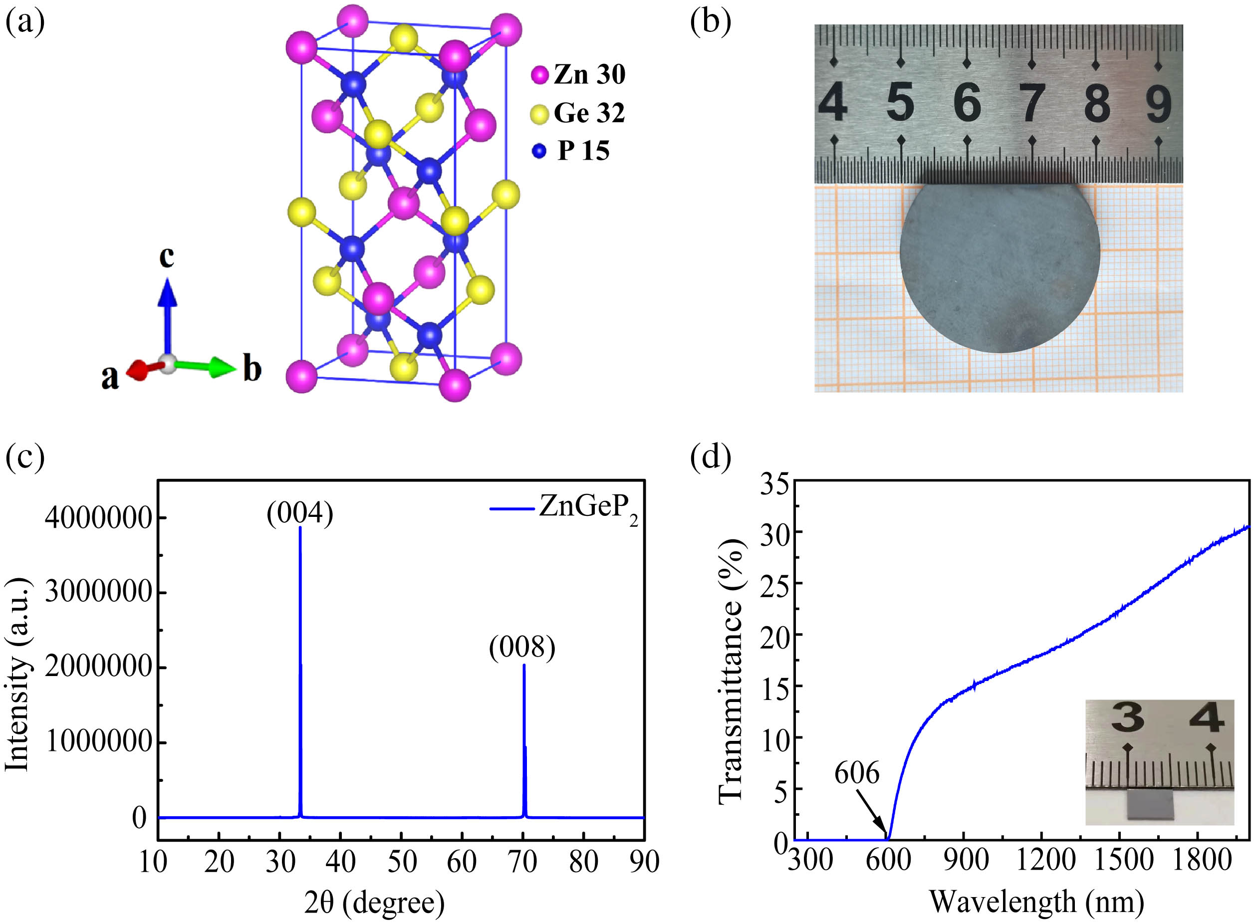
    Fig. 1. (a) Atomic model of a unit cell of a chalcopyrite ZGP crystal structure; pink, yellow, and blue balls denote Zn, Ge, and P atoms, respectively. (b) Photograph of ZGP wafer fabricated from as-grown ZGP single crystal; (c) XRD pattern of the (001) surface; (d) UV-Vis-NIR transmission spectrum of the ZGP crystal (Eg about 2.05 eV), whose photograph is shown in the inset.
    (a) HAADF-STEM images of a chalcopyrite ZGP nanoplate. Inset, FFT patterns of the (001) plane from the image. (b)–(j) Lattice line profiles of the ZGP nanoplate (001) plane. The zoomed HAADF-STEM images are processed to increase the contrast. The dashed rectangles with red, pink, orange, and light blue colors are marked on both the atomic models and corresponding zoomed STEM images to show the defects. The Zn vacancy, P vacancy, and GeZn antisite are shown in the STEM images marked with pink, yellow, and red open rings, respectively. (k) Large-scale atomic HAADF-STEM image. (l) STEM image (upper left) and corresponding STEM-EDS chemical maps. (m) STEM-EDS pattern of a ZGP nanoplate.
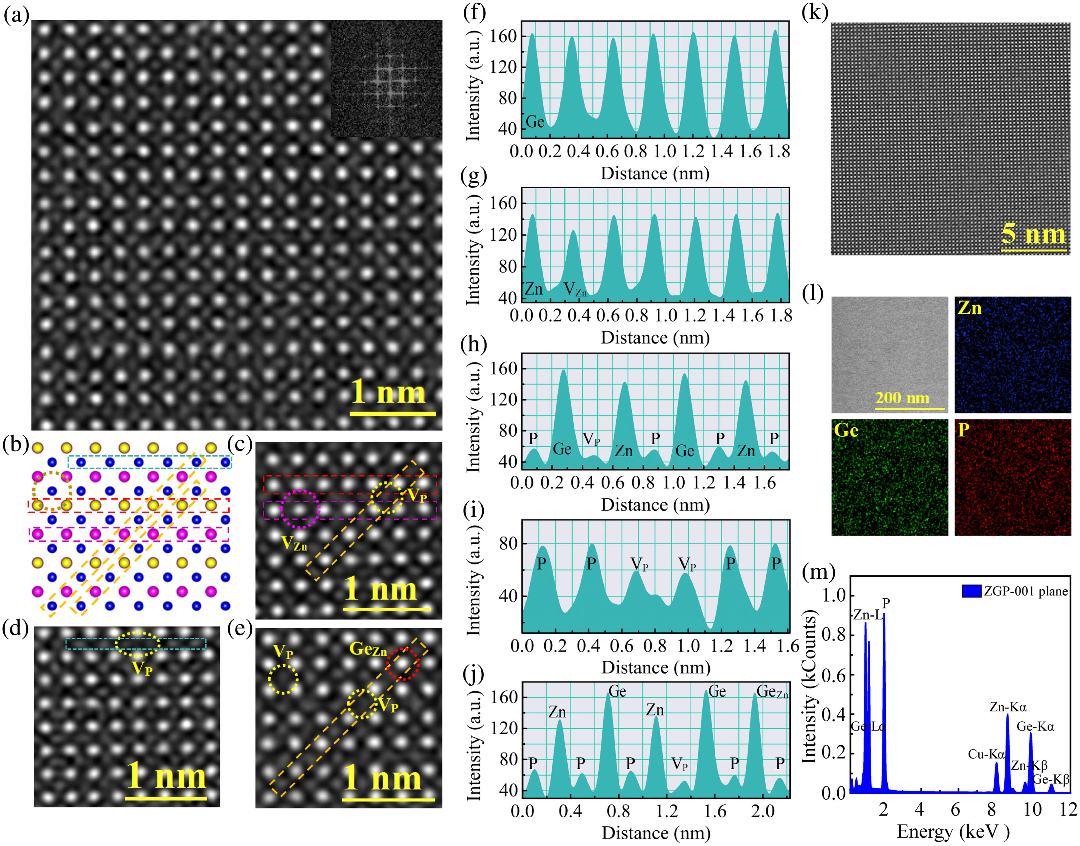
    Fig. 2. (a) HAADF-STEM images of a chalcopyrite ZGP nanoplate. Inset, FFT patterns of the (001) plane from the image. (b)–(j) Lattice line profiles of the ZGP nanoplate (001) plane. The zoomed HAADF-STEM images are processed to increase the contrast. The dashed rectangles with red, pink, orange, and light blue colors are marked on both the atomic models and corresponding zoomed STEM images to show the defects. The Zn vacancy, P vacancy, and GeZn antisite are shown in the STEM images marked with pink, yellow, and red open rings, respectively. (k) Large-scale atomic HAADF-STEM image. (l) STEM image (upper left) and corresponding STEM-EDS chemical maps. (m) STEM-EDS pattern of a ZGP nanoplate.
    (a) Raman spectra of a ZGP crystal at 77 and 300 K on the (001) plane; (b) PL spectra of the ZGP crystal at different temperatures; (c) the PL spectra are multiple-peak fitted at 77 K and 300 K. (d) Schematic band structures with dominant native defect levels for the ZGP crystal; (e) power-dependent PL spectra of the ZGP crystal at 77 K; (f) extracted PL intensities for point defects at 1.70, 1.59, 1.47, and 1.37 eV with the increasing excitation power.
    Fig. 3. (a) Raman spectra of a ZGP crystal at 77 and 300 K on the (001) plane; (b) PL spectra of the ZGP crystal at different temperatures; (c) the PL spectra are multiple-peak fitted at 77 K and 300 K. (d) Schematic band structures with dominant native defect levels for the ZGP crystal; (e) power-dependent PL spectra of the ZGP crystal at 77 K; (f) extracted PL intensities for point defects at 1.70, 1.59, 1.47, and 1.37 eV with the increasing excitation power.
    Schematic diagram of an ultrafast pump-probe spectroscopy system for the measurement of time-resolved reflectivity. R, reflector; BS, beam splitter; L1 and L2, lenses; YAG, yttrium aluminum garnet crystal; F, bandpass filter; MO, short-working-distance microscope objective; OPA, optical parametric amplifier; CMOS, complementary metal-oxide-semiconductor image sensor.
    Fig. 4. Schematic diagram of an ultrafast pump-probe spectroscopy system for the measurement of time-resolved reflectivity. R, reflector; BS, beam splitter; L1 and L2, lenses; YAG, yttrium aluminum garnet crystal; F, bandpass filter; MO, short-working-distance microscope objective; OPA, optical parametric amplifier; CMOS, complementary metal-oxide-semiconductor image sensor.
    (a) TR 2D contour plots of a ZGP crystal at delay times from 1 to 7000 ps with the fluence of 0.62 mJ/cm2 at 77 K; (b) dynamic decay curve extracted at 606.6 nm; the inset shows the rising time for this process. (c) Schematic mechanism of carrier dynamics stimulated by a 530 nm pump laser; (d) and (e) TR 2D contour plots and dynamic decay curve extracted at 606.6 nm at 300 K; (f) decay time constants τ with the pump fluences.
    Fig. 5. (a) TR 2D contour plots of a ZGP crystal at delay times from 1 to 7000 ps with the fluence of 0.62 mJ/cm2 at 77 K; (b) dynamic decay curve extracted at 606.6 nm; the inset shows the rising time for this process. (c) Schematic mechanism of carrier dynamics stimulated by a 530 nm pump laser; (d) and (e) TR 2D contour plots and dynamic decay curve extracted at 606.6 nm at 300 K; (f) decay time constants τ with the pump fluences.
    (a) TR spectra of a ZGP crystal with different delay times upon excitation with a 530 nm femtosecond laser; (b) dynamic decay curves of native point defects excited with a 530 nm femtosecond laser at 759.1, 734.1, and 840.1 nm; (c) dynamic decay curves of native point defects in early probe delays. The laser fluence is 0.62 mJ/cm2, and the temperature is 77 K.
    Fig. 6. (a) TR spectra of a ZGP crystal with different delay times upon excitation with a 530 nm femtosecond laser; (b) dynamic decay curves of native point defects excited with a 530 nm femtosecond laser at 759.1, 734.1, and 840.1 nm; (c) dynamic decay curves of native point defects in early probe delays. The laser fluence is 0.62 mJ/cm2, and the temperature is 77 K.
    Xiaoguang Pan, Yongzheng Wang, Hangxin Bai, Caixia Ren, Jiangbo Peng, Fangli Jing, Hailong Qiu, Zuotao Lei, Hongjun Liu, Chunhui Yang, Zhanggui Hu, Yicheng Wu. Atomic structures and carrier dynamics of defects in a ZnGeP2 crystal[J]. Chinese Optics Letters, 2023, 21(4): 041604
    Download Citation