• Chinese Optics Letters
  • Vol. 21, Issue 4, 041604 (2023)
Xiaoguang Pan1, Yongzheng Wang1, Hangxin Bai1, Caixia Ren1, Jiangbo Peng1, Fangli Jing1, Hailong Qiu1, Zuotao Lei2、*, Hongjun Liu1、**, Chunhui Yang2, Zhanggui Hu1, and Yicheng Wu1
Author Affiliations
  • 1Tianjin Key Laboratory of Functional Crystal Materials, Institute of Functional Crystals, School of Materials Science and Engineering, Tianjin University of Technology, Tianjin 300384, China
  • 2Harbin Institute of Technology, Harbin 150001, China
  • show less
    DOI: 10.3788/COL202321.041604 Cite this Article Set citation alerts
    Xiaoguang Pan, Yongzheng Wang, Hangxin Bai, Caixia Ren, Jiangbo Peng, Fangli Jing, Hailong Qiu, Zuotao Lei, Hongjun Liu, Chunhui Yang, Zhanggui Hu, Yicheng Wu. Atomic structures and carrier dynamics of defects in a ZnGeP2 crystal[J]. Chinese Optics Letters, 2023, 21(4): 041604 Copy Citation Text show less

    Abstract

    ZnGeP2 (ZGP) crystals have attracted tremendous attention for their applications as frequency conversion devices. Nevertheless, the existence of native point defects, including at the surface and in the bulk, lowers their laser-induced damage threshold by increasing their absorption and forming starting points of the damage, limiting their applications. Here, native point defects in a ZGP crystal are fully studied by the combination of high angle annular dark-field scanning transmission electron microscopy (HAADF-STEM) and optical measurements. The atomic structures of the native point defects of the Zn vacancy, P vacancy, and Ge-Zn antisite were directly obtained through an HAADF-STEM, and proved by photoluminescence (PL) spectra at 77 K. The carrier dynamics of these defects are further studied by ultrafast pump-probe spectroscopy, and the decay lifetimes of 180.49, 346.73, and 322.82 ps are attributed to the donor Vp+ → valence band maximum (VBM) recombination, donor GeZn+ → VBM recombination, and donor–acceptor pair recombination of Vp+ → VZn-, respectively, which further confirms the assignment of the electron transitions. The diagrams for the energy bands and excited electron dynamics are established based on these ultrahigh spatial and temporal results. Our work is helpful for understanding the interaction mechanism between a ZGP crystal and ultrafast laser, doing good to the ZGP crystal growth and device fabrication.

    1. Introduction

    Zinc-germanium-phosphorus (ZnGeP2, or ZGP), a II-IV-V2 ternary chalcopyrite structure crystal with a pseudodirect bandgap of 2.1eV, is the most highly efficient nonlinear optical crystal for laser frequency conversion in the middle infrared region[13]. It has a unique set of optical and nonlinear optical properties, such as wide transmission range (0.7–12 µm), large nonlinear coefficient (d36=75pm/V), high thermal conductivity (360mW·cm1·K1), an applicable laser-induced damage threshold (30GW/cm2), and suitable birefringence (0.040–0.042)[46]. As an essential laser frequency conversion crystal, ZGP can be widely used for the generation of infrared optical parametric oscillation (OPO), optical parametric amplifier (OPA), frequency mixing (FM), and second-harmonic generation (SHG)[710]. Pumped at 2 µm, the ZGP OPO can realize continuously tunable laser output in the range of 3–8 µm with a conversion efficiency of more than 50%[11]. In addition, it also has important and prospective applications in many fields, such as spectroscopy, atmospheric detection, medical treatment, environmental protection, and military field[3,12,13].

    With the development of high-power infrared laser and optical devices based on the ZGP crystal, its laser-induced damage threshold limits its further application. The defects in this crystal were believed to be one of the key problems for its relatively low laser-induced damage threshold. Although this material is relatively transparent in the region of 0.7–2.5 µm, there is still a wide range of defect absorption-related absorption bands[11,1416]. These resulting absorption bands seriously reduce the application performance of the OPO. Similarly, it has deep absorption near 1 µm and low absorption near 2 µm, which is related to native point defects[11,17]. The existence of the point defects in a ZGP crystal destroys the periodic potential field of the crystal and affects binding energies, spatial distribution, and mobility of the electrons. These effects thus change the energy bands near the defects, strongly affecting the optical, thermal, electrical, and magnetic properties of the crystal. Furthermore, the surface defects caused from the crystal growth and processing strongly affect the interaction between the incident laser and the crystal. The surface defects are easily destroyed after absorbing the incident laser due to their abundant defect states and then become the beginning of the coming heavier damage[1820]. Thus, how to decrease the defect density in a ZGP crystal has already been the most critical bottleneck in restricting its practical applications. Studying the atomic structures of defects and carrier dynamics during the interaction between the defects and incident laser is one of the key problems for enhancing the damage threshold for a ZGP crystal.

    It is revealed that the dominant acceptor was the singly ionized zinc vacancy in a ZGP crystal by electron paramagnetic resonance (EPR) and electron-nuclear double resonance (ENDOR)[11,21], and the existence of zinc vacancy in ZGP crystal was further confirmed by positron annihilation lifetime (PAL) spectroscopy[22]. Photoluminescence (PL) spectra of a ZGP crystal suggested that the luminescence of defects was related to P vacancy[23,24]. Optically detected magnetic resonance (ODMR) tests demonstrated that three different native defects (Ge-Zn antisite, Zn and P vacancies) can contribute to the absorption in a ZGP crystal[15]. Up to now, the atomic structures of native point defects in ZGP crystals have not been resolved, and the electronic dynamics around the defects have not been studied. The state-of-the-art characterization techniques, such as spherical aberration-corrected scanning transmission electron microscopy (Cs-STEM) and ultrafast pump-probe spectroscopy, can help us gain insight into the atomic structures at atomic scale and probe the electronic dynamics at femtosecond scale[25,26], which provides a novel way to study the native defects of a ZGP crystal. Point defects in crystals can be observed through a Cs-STEM after being thinned to a certain thickness by focused ion beam (FIB) technology. A strong current ion beam peels the atoms on the crystal surface, which does little damage to the original crystal structure. This will enable the point defects of crystals to be visualized by a Cs-STEM[27,28].

    In this work, the native point defects, both at the surface and in the bulk, of a ZGP crystal are studied by combining Cs-STEM and ultrafast pump-probe spectroscopy. Three types of native point defects in ZGP crystal are found by the Cs-STEM and confirmed by PL spectra at 77 K. The electronic dynamics of these defects are further studied by ultrafast pump-probe spectroscopy. The direct visualization of such native defects will benefit the crystal growth and device fabrication of ZGP crystals.

    2. Experimental Details

    2.1. Preparation of a ZGP crystal

    The cut slice of the ZGP crystal with the diameter of 30 mm was used for X-ray diffraction (XRD) measurement. A ZGP crystal with the size of 5.0mm×5.0mm×0.5mm was cut and polished, and the incident direction was normal to the (001) plane. The well-polished crystals were used for the measurements, such as UV-Vis-NIR transmission spectrum, PL spectrum, Raman spectrum, and ultrafast pump-probe spectroscopy. To get the atomic structures of ZGP, a ZGP nanoplate orientated normal to the (001) face with the size of 50 nm was fabricated by focused ion beam-scanning electron microscopy (FIB-SEM) system to be measured by a spherical aberration Cs-STEM. The percentage of chemical element content was measured by scanning transmission electron microscopy equipped with energy dispersive X-ray spectroscopy (STEM-EDS).

    2.2. Characterization

    XRD measurement was performed using a SmartLab 9 kW X-ray diffractometer at room temperature with CuKα radiation in the scanning range of 10°–90°. Atomic structures of the ZGP crystal were obtained using a spherical aberration Cs-STEM (Titan Themis Cubed G2 60-300). The UV-Vis-NIR transmission spectrum (UH4150) was used to characterize the bandgap energy (Eg) of a ZGP crystal. In addition, PL and Raman spectra were collected on a 0.5 mm-thick ZGP crystal using a confocal Raman microscopic system (WITec Alpha 300RA) with a 532 nm laser. Temperature-dependent PL spectra of ZGP crystal were collected from 77 to 297 K.

    The carrier dynamics were studied on a polished ZGP crystal of 5.0mm×5.0mm×0.5mm with the incident direction normal to the (001) plane. Transient reflection (TR) spectra were collected using a home-built micro-ultrafast pump-probe system. A Yb:KGW laser (Pharos, Light Conversion Ltd.) at 1030 nm (repetition rate, 100 kHz; pulse width, 120 fs) was employed as the radiation source, which was split into two beams. One was directed into an OPA to generate a pump pulse (315–2600 nm), while the other passed through a time delay line and then hit on an yttrium aluminum garnet (YAG) crystal to produce white supercontinuum light as the probe pulse. Then, the pump and probe beams were collinearly focused onto the ZGP crystal with a 60× objective lens. The reflection signals from the sample were collected by a complementary metal-oxide-semiconductor (CMOS) detector after the pump pulse was filtered with a long-wave pass filter. The TR signal was calculated as ΔR/R0=(Rpump-onRpump-off)/Rpump-off, where Rpump-on and Rpump-off are the reflected probe signals with and without the pump excitation. To study the time-resolved dynamics of the ZGP crystal, the TR measurements were performed under a 530 nm pump femtosecond laser at 300 and 77 K.

    3. Results and Discussion

    3.1. XRD and UV-Vis-NIR transmission analysis

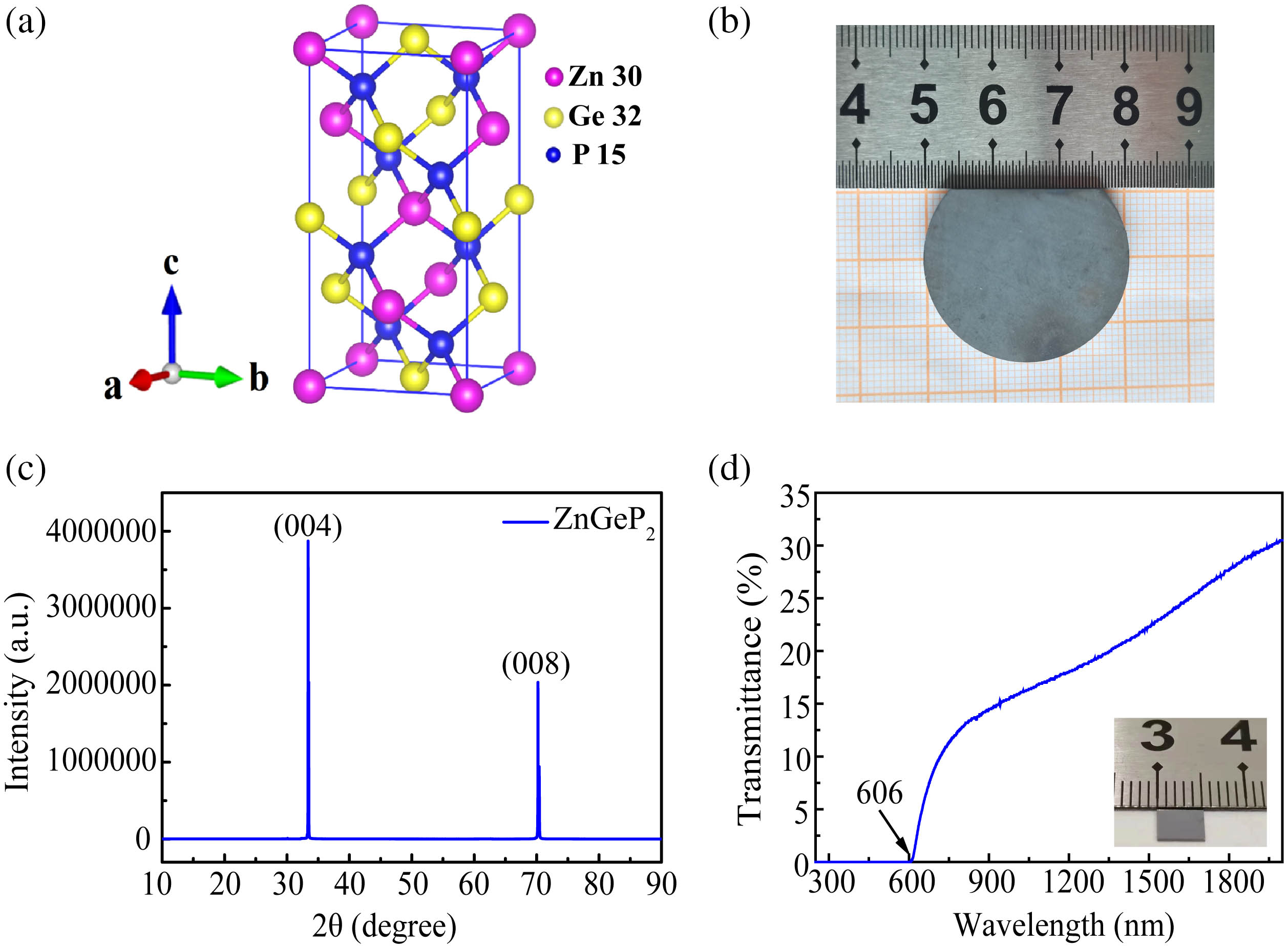
    The atomic models for a chalcopyrite ZGP crystal are shown in Fig. 1(a), in which pink, yellow, and blue balls correspond to Zn, Ge, and P atoms, respectively. The tetrahedron formed by Zn, Ge, and P atoms constitutes the basic structural unit of the ZGP crystal, with the lattice constants of a=b=0.5454nm, c=1.0707nm, and α=β=γ=90°[29]. The four vertex positions of the tetrahedron are occupied by Zn2+ and Ge4+ cations, respectively, while the anion P3 is located in the center of the tetrahedron. In the structure, the bond lengths of Zn-P in [ZnP4] and Ge-P in [GeP4] tetrahedron are 0.2379 and 0.2328 nm[30], respectively. The radius difference of these two cations and the distinct interaction force among these two cations and anions make the crystal structure of ZGP slightly deformed on the basis of sphalerite structure, leading to an irregular tetrahedron. A ZGP crystal with the diameter of 30 mm was grown by a vertical Bridgman technique[31]; the cut slice of the crystal is shown in Fig. 1(b). The XRD spectrum was collected on the slice, shown in Fig. 1(c). The high intensity and narrow full width at half-maximum (FWHM) of two peaks (004) and (008) illustrate the high quality of the ZGP crystal. A UV-Vis-NIR transmission spectrum was collected on a polished ZGP crystal with the size of 5.0mm×5.0mm×0.5mm using a UH-4150 spectrophotometer, shown in Fig. 1(d). The absorption edge of the crystal is near 606 nm (2.05 eV), agreeing with the previously reported experimental value of 2.02 eV[2].

    (a) Atomic model of a unit cell of a chalcopyrite ZGP crystal structure; pink, yellow, and blue balls denote Zn, Ge, and P atoms, respectively. (b) Photograph of ZGP wafer fabricated from as-grown ZGP single crystal; (c) XRD pattern of the (001) surface; (d) UV-Vis-NIR transmission spectrum of the ZGP crystal (Eg about 2.05 eV), whose photograph is shown in the inset.

    Figure 1.(a) Atomic model of a unit cell of a chalcopyrite ZGP crystal structure; pink, yellow, and blue balls denote Zn, Ge, and P atoms, respectively. (b) Photograph of ZGP wafer fabricated from as-grown ZGP single crystal; (c) XRD pattern of the (001) surface; (d) UV-Vis-NIR transmission spectrum of the ZGP crystal (Eg about 2.05 eV), whose photograph is shown in the inset.

    3.2. HAADF-STEM analysis

    The HAADF-STEM images were collected on a ZGP nanoplate with a thickness of less than 50 nm, shown in Fig. 2. A large-scale atomic HAADF-STEM image for the (001) plane of a ZGP nanoplate shows that there are no obvious lattice dislocations in this region [Figs. 2(a) and 2(k)]. Figure 2(a) shows a zoomed HAADF-STEM image with atomic structures of the (001) plane, and the corresponding fast Fourier transform (FFT) pattern is listed in the inset. Considering the difference of the atomic numbers, two rows of bright spots are suggested to be heavier Ge(32) and Zn(30) atoms, while the dim dots are suggested to be P(15) atoms. By comparing the HAADF-STEM images with the atomic models, the atomic structures of native defects of the ZGP nanoplate are identified, as shown in Figs. 2(b)2(j). The line profiles in Figs. 2(f)2(h) show the intensities of the corresponding atoms marked with red, pink, and orange dashed rectangles in Fig. 2(c). Due to the larger atomic number of Ge, the line profiles in Figs. 2(f) and 2(g) are believed to be from Ge atoms and Zn atoms, respectively. In addition, the line profile in Fig. 2(h) shows the atomic arrangement of P-Ge-P-Zn, marked with an oblique orange dashed rectangle. The intensity of the Zn atoms marked by the pink dashed line is significantly different in Fig. 2(g), while the intensity of the Ge atoms marked with a red dashed line shows little change in Fig. 2(f). This indicates that there is a zinc vacancy (VZn) defect in the spot marked with a big pink dotted circle in Fig. 2(c). Similarly, the presence of phosphorus vacancy defects (VP) was determined by significant intensity differences in Fig. 2(h), marked with a small yellow dotted circle. The existence of VP defects is further confirmed by the HAADF-STEM image and line profile in Figs. 2(d), 2(e), 2(i), and 2(j), which are marked with yellow dotted ovals and circles in the corresponding positions in the HAADF-STEM images. Along the oblique dashed rectangle in Figs. 2(e) and 2(j), an antisite defect (GeZn) is revealed, marked with a dashed (red) circle in the HAADF-STEM image. It should be noted that the thickness of the nanoplate is about 50 nm, so the intensities of the HAADF-STEM are from nearly 100 atoms in each position. Thus, the absence of a single atom cannot be directly shown in our HAADF-STEM images, which can only be revealed by the intensity difference at different positions. To exclude the effects from the impurity, scanning transmission electron microscopy (STEM)-energy dispersive X-ray spectroscopy (STEM-EDS) measurements were performed on the (001) plane; the EDS maps and curves of Zn, Ge, and P elements are shown in Fig. 2(l). It can be seen that Zn, Ge, and P atoms are evenly distributed on the (001) plane. In addition, the atomic percentages of Zn, Ge, and P presented by STEM-EDS are 27.24%, 23.81%, and 48.96%, respectively, which is very close to the stoichiometric formula [Fig. 2(m)]. No impurity elements are found on the tested sample, indicating that these defects are native defects for the ZGP nanoplate.

    (a) HAADF-STEM images of a chalcopyrite ZGP nanoplate. Inset, FFT patterns of the (001) plane from the image. (b)–(j) Lattice line profiles of the ZGP nanoplate (001) plane. The zoomed HAADF-STEM images are processed to increase the contrast. The dashed rectangles with red, pink, orange, and light blue colors are marked on both the atomic models and corresponding zoomed STEM images to show the defects. The Zn vacancy, P vacancy, and GeZn antisite are shown in the STEM images marked with pink, yellow, and red open rings, respectively. (k) Large-scale atomic HAADF-STEM image. (l) STEM image (upper left) and corresponding STEM-EDS chemical maps. (m) STEM-EDS pattern of a ZGP nanoplate.

    Figure 2.(a) HAADF-STEM images of a chalcopyrite ZGP nanoplate. Inset, FFT patterns of the (001) plane from the image. (b)–(j) Lattice line profiles of the ZGP nanoplate (001) plane. The zoomed HAADF-STEM images are processed to increase the contrast. The dashed rectangles with red, pink, orange, and light blue colors are marked on both the atomic models and corresponding zoomed STEM images to show the defects. The Zn vacancy, P vacancy, and GeZn antisite are shown in the STEM images marked with pink, yellow, and red open rings, respectively. (k) Large-scale atomic HAADF-STEM image. (l) STEM image (upper left) and corresponding STEM-EDS chemical maps. (m) STEM-EDS pattern of a ZGP nanoplate.

    3.3. Raman and PL analysis

    Raman spectra were collected on a polished ZGP crystal at 300 and 77 K, as shown in Fig. 3(a). The ZGP crystal has a body-centered tetragonal cell with a space group of I4¯2d. The characteristic of its point group 4¯2m indicates the symmetry of lattice vibration, having nondegenerate A1, A2, B1, and B2 modes and a doubly degenerated E mode. These modes, A1, A2, B1, B2, and E, are Raman-activated with quadratic basis functions. Raman modes B2 and E have linear basis functions as dipole moment transformation, so they exhibit longitudinal optical (LO) and transverse optical (TO) splitting[32]. Three peaks with strong intensities are found at 329, 360, and 412cm1, corresponding to A1 and B2 (LO) phonon vibration modes in ZGP, respectively. Similarly, three weak Raman peaks are also observed between the E (TO) mode (248cm1), E (LO) mode (391cm1), and B1 mode (122cm1), agreeing with the reported Raman vibration mode of the ZGP crystal[32,33]. The Raman spectrum collected at 77 K is identical to those at 300 K, indicating that there is no phase transition during the cooling.

    (a) Raman spectra of a ZGP crystal at 77 and 300 K on the (001) plane; (b) PL spectra of the ZGP crystal at different temperatures; (c) the PL spectra are multiple-peak fitted at 77 K and 300 K. (d) Schematic band structures with dominant native defect levels for the ZGP crystal; (e) power-dependent PL spectra of the ZGP crystal at 77 K; (f) extracted PL intensities for point defects at 1.70, 1.59, 1.47, and 1.37 eV with the increasing excitation power.

    Figure 3.(a) Raman spectra of a ZGP crystal at 77 and 300 K on the (001) plane; (b) PL spectra of the ZGP crystal at different temperatures; (c) the PL spectra are multiple-peak fitted at 77 K and 300 K. (d) Schematic band structures with dominant native defect levels for the ZGP crystal; (e) power-dependent PL spectra of the ZGP crystal at 77 K; (f) extracted PL intensities for point defects at 1.70, 1.59, 1.47, and 1.37 eV with the increasing excitation power.

    PL spectra were measured under the excitation of a 532 nm laser. Figure 3(b) shows the temperature-dependent PL spectra of a ZGP crystal from 77 to 297 K. The PL spectra at different temperatures reveal that the ZGP crystal has broadband emission in the range of 650 to 1050 nm, and the maximum intensity varies in the range of 700 to 800 nm[34]. The enhanced intensity and unshifted prominent peaks by decreasing the temperature from 297 to 77 K indicate that the PL spectra are related to the native defects in the ZGP crystal. As the temperature decreases, the defect-bound excitons become stabler, while the phonon-assisted nonradiative transition in the crystal decreases, resulting in the sharp enhancement of PL intensity[35]. The broad defect emission bands suggest that multiple defect bands contribute to the subbandgap. It can be seen that the bandgap emission is absent in the PL spectra, confirming pseudo-direct bandgap semiconductor characteristic of ZGP crystals.

    To understand the origin of the defect luminescence, the individual bands were extracted with a multipeak Gaussian fitting from the obtained PL spectra. At 77 K, the PL spectrum can be fitted into four peaks with the central peaks located at 1.70, 1.59, 1.47, and 1.37 eV, while these four peaks are located at 1.68, 1.59, 1.47, and 1.36 eV at 300 K [Fig. 3(c)]. These fitted peaks are believed to correspond to the radiative transition among different defects. Considering the error during the fitting, the fitted results indicate that the temperature has little effect on the radiative emission. According to the Varshni empirical relationship[36], the bandgap of a semiconductor varies with the temperature, Eg(T)=E0αT2/(T+β),where E0 is the width of the bandgap at zero temperature, and α and β are empirical parameters that have no concrete physical significance. Nevertheless, the binding energies of defect-bounded excitons are almost independent of the temperature. Thus, the invariant central peak positions of PL with decreasing temperature demonstrate the obtained PL spectra are from the defects, rather than from the bandgap emission.

    Combined with the reported results from photo-EPR, EPR, and PL at 15 and 5 K, the corresponding electronic transitions for the PL peaks are identified. It is reported that the photo-induced recharging level was connected with the Ge antisite donor defect GeZn+ at 1.70 eV[37], so the PL peak located at 1.70 eV can be attributed to the Ge antisite donor defect level GeZn+. The correlation between EPR and PL showed that the 1.58 eV band was enhanced in ZGP samples with a higher concentration of phosphorus vacancy (VP)[23,24]. PL measurements further confirmed the assignment of the emission band of 1.6 eV to the donor (VP+)VBM (D, hole) recombination, while another PL emission band near 1.4 eV was attributed to donor–acceptor pair (DAP) recombination, i.e., VP+VZn[38]. In addition, the band located at about 1.36 eV (911.8 nm) was referred to as the “low-energy band” (LEB)[23]. The 1.36 eV PL band is most likely due to radiative transitions between the VP electron states and VBM. The VP electron states are obtained by the electron transfer of the VP+(singly ionized states)VP0(neutral states)VP (negatively charged states) process. With the reported results from the EPR and PL measurements, these four PL peaks are attributed to the emission related to the native defects in the ZGP crystal by combining the atomic results from HAADF-STEM measurements in Fig. 2. The peaks located at 1.70, 1.59, 1.47, and 1.37 eV are assigned to the donor (GeZn+)VBM (D, hole) recombination, donor (VP+)VBM (D, hole) recombination, donor (VP+)–acceptor (VZn) pair (DAP) recombination, and acceptor (VP)VBM recombination. Based on the above understandings, the schematic band structure near the Fermi surface for the ZGP crystal is summarized in Fig. 3(d).

    Power-dependent PL spectra of the ZGP crystal were also collected at 77 K, listed in Fig. 3(e), in which PL intensities increase with increasing incident laser power density. The power-dependent peak intensities at 1.70, 1.59, 1.47, and 1.37 eV are extracted from the fitted PL spectra, shown in Fig. 3(f). It is obvious that there are two kinds of power dependence in this chart. For the transitions, such as donor (GeZn+)VBM (D, hole) recombination, donor (VP+)VBM (D, hole) recombination, and DAP recombination, the PL intensities increase sharply with the increasing excitation power and nearly reach saturation at the maximum excitation power. On the other hand, the PL intensity for the acceptor (VP)VBM recombination quickly reaches its saturation by increasing the excitation power at a much lower level. This behavior can be interpreted by the excited carriers for the PL radiation in different transitions. For the former three transitions, the excited carriers are formed from the relaxed hot electrons from the conduction band minimum (CBM), which is nearly linear to the incident laser power at the beginning and saturates at some high laser power. Nevertheless, in the later transitions, the concentration of the acceptor (VP) is strongly dependent on the concentrations of VP0 and VP+[24], which are heavily decreased by the three former transitions. These different power dependences prove the schematic band structures in Fig. 3(d).

    3.4. Ultrafast carrier dynamics analysis

    The excited carrier dynamics are further studied by an ultrafast pump-probe spectroscopy system, shown in Fig. 4. This system mainly includes a femtosecond laser, delay time control system, microscopy, and high-sensitivity detector. More details about this system are described in Section 2. The TR spectra were measured by ultrafast pump-probe technology under a 530 nm femtosecond laser with the fluence of 0.62mJ/cm2 at 77 and 300 K; the corresponding 2D contour plots of the TR spectra are shown in Figs. 5(a) and 5(d), respectively. Then, the dynamic process of excited hot carriers is obtained by analyzing the transient reflectivity variation. For consistency, exponentially fitting is employed to get the decay lifetime τ of the dynamic decay curve[39]. The decay dynamic curves at the wavelength of 606.6 nm, the wavelength for the indirect bandgap, are extracted from the 2D contour plots in Figs. 5(a) and 5(d), and listed in Figs. 5(b) and 5(e), respectively. The fitted lifetime τ is 103.57 ps at 77 K and 293.36 ps at 300 K, respectively. Within the first picosecond after being irradiated by a femtosecond laser, electrons in the crystal absorb the incident energy higher than the bandgap and are heated to a higher energy level. Subsequently, the excited hot electrons rapidly relax to the CBM; then the relaxed electrons transit to the ground level by indirect transition with the assistance of electron-phonon scattering[40,41], as schematically shown in Fig. 5(c). The carrier dynamics were further studied at various temperatures (77 and 300 K) and under various excitation fluences. The fitted decay lifetimes at different pump fluences at 77 and 300 K are shown in Fig. 5(f), indicating that there is a relatively shorter decay time constant τ at the low temperature of 77 K. As the temperature increases from 77 to 300 K, the speedup of nonradiative recombination will decrease the PL intensity, while the increasing electron-phonon scattering extends the decay lifetime τ, resulting in a larger decay lifetime[42]. With the increasing excitation fluence at the same temperature, the enhanced Auger recombination from the increasing carriers’ population shortens the decay time τ, as shown in Fig. 5(f)[43]. At 300 K, electron-phonon scattering is much more significant, owing to more phonons than those at 77 K. Therefore, due to the stronger electron-phonon scattering, the decrease of the decay lifetime at 300 K is not so sensitive as that at 77 K.

    Schematic diagram of an ultrafast pump-probe spectroscopy system for the measurement of time-resolved reflectivity. R, reflector; BS, beam splitter; L1 and L2, lenses; YAG, yttrium aluminum garnet crystal; F, bandpass filter; MO, short-working-distance microscope objective; OPA, optical parametric amplifier; CMOS, complementary metal-oxide-semiconductor image sensor.

    Figure 4.Schematic diagram of an ultrafast pump-probe spectroscopy system for the measurement of time-resolved reflectivity. R, reflector; BS, beam splitter; L1 and L2, lenses; YAG, yttrium aluminum garnet crystal; F, bandpass filter; MO, short-working-distance microscope objective; OPA, optical parametric amplifier; CMOS, complementary metal-oxide-semiconductor image sensor.

    (a) TR 2D contour plots of a ZGP crystal at delay times from 1 to 7000 ps with the fluence of 0.62 mJ/cm2 at 77 K; (b) dynamic decay curve extracted at 606.6 nm; the inset shows the rising time for this process. (c) Schematic mechanism of carrier dynamics stimulated by a 530 nm pump laser; (d) and (e) TR 2D contour plots and dynamic decay curve extracted at 606.6 nm at 300 K; (f) decay time constants τ with the pump fluences.

    Figure 5.(a) TR 2D contour plots of a ZGP crystal at delay times from 1 to 7000 ps with the fluence of 0.62 mJ/cm2 at 77 K; (b) dynamic decay curve extracted at 606.6 nm; the inset shows the rising time for this process. (c) Schematic mechanism of carrier dynamics stimulated by a 530 nm pump laser; (d) and (e) TR 2D contour plots and dynamic decay curve extracted at 606.6 nm at 300 K; (f) decay time constants τ with the pump fluences.

    Finally, the carrier dynamics for these defects in a ZGP crystal are further studied by the ultrafast pump-probe spectroscopy. TR spectra and decay curves of native point defects are extracted from the 2D contour plot in Fig. 5(a) under a laser fluence 0.62mJ/cm2 at 77 K, as shown in Figs. 6(a) and 6(b), respectively. The TR spectra with peak positions located at 759.1 nm (1.63 eV), 734.1 nm (1.69 eV), and 840.1 nm (1.48 eV) are shown in Fig. 6(a). To show the maximum intensity, these TR spectra are extracted at different delay times of 1.5, 3.7, and 36.2 ps, respectively. According to the PL spectra in Fig. 3, they can be attributed to the transitions of donor defect VP+VBM, donor defect GeZn+VBM, and DAP recombination due to VP+VZn, respectively. The corresponding decay curves of the point defects under the excitation of a 530 nm femtosecond laser are shown in Fig. 6(b). These decay curves are adequately fitted by a single exponential function, giving the lifetimes of τ1=180.49ps, τ2=346.73ps, and τ3=322.82ps, respectively. It is worth noting that the lifetimes for the donor GeZn+VBM and DAP recombination are roughly similar, while the lifetime for donor VP+VBM recombination is relatively shorter. During the excitation, the electrons with the ground states are pumped into the CB, and then fast-relaxed to the donor states (GeZn+ and VP+). This process is very fast, with decay times of several picoseconds, which are shown as the rising times with the separations between the blue and red dashed lines in Fig. 6(c). Then the hot electrons transit from the donor states to the lower energy levels with radiation. In Fig. 6(c), the rising times, corresponding to the relaxation process from the excited hot electrons to donor energy level, are nearly the same for the donor GeZn+VBM and donor VP+VBM recombination. It should be noted that the rising time for the DAP recombination is about 1.5 times larger than those of the former two. The longer rising time suggests that there should be a process from VP+ to VP0 that increases the hot electrons’ relaxation time. It should be noted that the rising time for all these three processes is much shorter than that for the indirect transition in Fig. 5(b). The indirect relaxation to CBM includes the electron intervalley scattering, which prolongs the rising time in Fig. 5(b). On the other hand, since the defect states are dispersionless, the electrons at the CBM can transit to the defect states without the scattering, which will shorten the corresponding rising time in Fig. 6(c). For the processes about the recombination, both the donor GeZn+VBM and DAP VP+VZn have nearly the same lifetimes, since the hot electrons hop among different atom sites, while the lifetime for the donor VP+VBM recombination is much shorter than those of the other two transitions. The transient spectra further confirmed the assignment of the PL peaks in Fig. 3. Unfortunately, the electron dynamics for the transition with the peak position located at 1.37 eV have not been studied, since it is out of the detection wavelength range of our home-built ultrafast pump-probe system. It should be noted that all the three lifetimes for the radiative recombination are a little larger than the decay lifetimes for indirect transitions. The unusual shorter indirect transition lifetimes suggested that there must be plenty of defect-assisted annihilation channels from the CBM to VBM. The massive annihilation processes transfer the energy from the hot electrons to the lattice and heat the lattice quickly, bringing the laser-induced damage.

    (a) TR spectra of a ZGP crystal with different delay times upon excitation with a 530 nm femtosecond laser; (b) dynamic decay curves of native point defects excited with a 530 nm femtosecond laser at 759.1, 734.1, and 840.1 nm; (c) dynamic decay curves of native point defects in early probe delays. The laser fluence is 0.62 mJ/cm2, and the temperature is 77 K.

    Figure 6.(a) TR spectra of a ZGP crystal with different delay times upon excitation with a 530 nm femtosecond laser; (b) dynamic decay curves of native point defects excited with a 530 nm femtosecond laser at 759.1, 734.1, and 840.1 nm; (c) dynamic decay curves of native point defects in early probe delays. The laser fluence is 0.62 mJ/cm2, and the temperature is 77 K.

    4. Conclusion

    In summary, the native point defects in a ZGP crystal, both at the surface and in the bulk, are fully studied with ultrahigh spatial and temporal resolutions. The HAADF-STEM images show that there are three kinds native point defects in the ZGP crystal, including VZn defects, GeZn antisite defects, and Vp defects. The fitted PL spectra reveal four defect bands, which are assigned to the donor (VP+)VBM (D, hole) recombination at 1.59 eV, donor (GeZn+)VBM (D, hole) recombination at 1.70 eV, acceptor (VP)VBM recombination at 1.37 eV, and VP+VZn DAP recombination band at 1.47 eV. This further confirms the primary point defects in the ZGP crystal, acceptor defects VZn, donor defects GeZn, and Vp observed by the HAADF-STEM. The TR spectra at 77 K present identical peaks to the PL spectra, and the fitted decay curves give the corresponding lifetimes of 180.49, 346.73, and 322.82 ps. With the above studies, we gain insight into native point defects with ultrahigh spatial and temporal resolution and establish clear diagrams for the energy bands and transition dynamics for the native defects in a ZGP crystal. Especially, the elucidation of the donor–acceptor recombination with long decay lifetimes can explain the reported coexistence of both a high density of point defects and high resistance. Our work can give a better comprehension of the mechanism for the interaction between a ZGP crystal and intense ultrafast laser, which might promote the applications of the IR intense ultrafast laser. Additionally, our work opens a new way to study the native defects of semiconducting crystals with ultrahigh temporal and spatial resolution.

    References

    [1] J. L. Shay, J. H. Wernick. Ternary Chalcopyrite Structure Semiconductors(1976).

    [2] X. Zhao, S. F. Zhu, B. J. Zhao, B. J. Chen, Z. Y. He, R. L. Wang, H. G. Yang, Y. Q. Sun, J. Cheng. Growth and characterization of ZnGeP2 single crystals by the modified Bridgman method. J. Cryst. Growth., 311, 190(2008).

    [3] L. Wang, T. L. Xing, S. W. Hu, X. Y. Wu, H. X. Wu, J. Y. Wang, H. H. Jiang. Mid-infrared ZGP-OPO with a high optical-to-optical conversion efficiency of 75.7%. Opt. Express, 25, 3373(2017).

    [4] D. H. Yang, B. J. Zhao, B. J. Chen, S. F. Zhu, Z. Y. He, W. Huang, Z. R. Zhao, M. D. Liu. Impurity phases analysis of ZnGeP2 single crystal grown by Bridgman method. J. Alloy. Compd., 709, 125(2017).

    [5] D. N. Nikogosyan. Nonlinear Optical Crystals: A Complete Survey(2006).

    [6] V. G. Dmitriev, G. G. Gurzadyan, D. N. Nikogosyan. Handbook of Nonlinear Optical Crystals(2013).

    [7] P. B. Phua, K. S. Lai, R. F. Wu, T. C. Chong. High-efficiency mid-infrared ZnGeP2 optical parametric oscillator in a multimode-pumped tandem optical parametric oscillator. Appl. Opt., 38, 563(1999).

    [8] C. P. Qian, X. M. Duan, B. Q. Yao, Y. J. Shen, Y. Zhang, B. R. Zhao, J. H. Yuan, T. Y. Dai, Y. L. Ju, Y. Z. Wang. 11.4 W long-wave infrared source based on ZnGeP2 optical parametric amplifier. Opt. Express, 26, 30195(2018).

    [9] U. Chatterjee. Development of coherent tunable source in 2–16 µm region using nonlinear frequency mixing processes. Pramana-J. Phys., 82, 29(2014).

    [10] L. V. Koval’chuk, A. N. Grezev, V. G. Niz’ev, V. P. Yakunin, V. S. Mezhevov, D. A. Goryachkin, V. V. Sergeev, A. G. Kalintsev. Repetitively pulsed TEA CO2 laser and its application for second harmonic generation in ZnGeP2 crystal. Quantum. Electron., 45, 884(2015).

    [11] S. D. Setzler, P. G. Schunemann, T. M. Pollak, M. C. Ohmer, J. T. Goldstein, F. K. Hopkins, K. T. Stevens, L. E. Halliburton, N. C. Giles. Characterization of defect-related optical absorption in ZnGeP2. J. Appl. Phys., 86, 6677(1999).

    [12] S.-H. Nam, V. Fedorov, S. Mirov, K.-H. Hong. Octave-spanning mid-infrared femtosecond OPA in a ZnGeP2 pumped by a 2.4 µm Cr:ZnSe chirped-pulse amplifier. Opt. Express, 28, 32403(2020).

    [13] T. T. Yu, S. P. Wang, X. Zhang, C. N. Li, J. Qiao, N. Jia, B. Han, S.-Q. Xia, X. T. Tao. MnSiP2: a new Mid-IR ternary phosphide with strong SHG effect and ultrabroad transparency range. Chem. Mater., 31, 2010(2019).

    [14] S. D. Setzler, N. C. Giles, L. E. Halliburton, P. G. Schunemann, T. M. Pollak. Electron paramagnetic resonance of a cation antisite defect in ZnGeP2. Appl. Phys. Lett., 74, 1218(1999).

    [15] D. M. Hofmann, N. G. Romanov, W. Gehlhoff, D. Pfisterer, B. K. Meyer, D. Azamat, A. Hoffmann. Optically detected magnetic resonance experiments on native defects in ZnGeP2. Physica B Condens. Matter, 340, 978(2003).

    [16] G. D. Zhang, X. T. Tao, S. P. Wang, G. D. Liu, Q. Shi, M. H. Jiang. Growth and thermal annealing effect on infrared transmittance of ZnGeP2 single crystal. J. Cryst. Growth., 318, 717(2011).

    [17] N. C. Giles, L. H. Bai, M. M. Chirila, N. Y. Garces, K. T. Stevens, P. G. Schunemann, S. D. Setzler, T. M. Pollak. Infrared absorption bands associated with native defects in ZnGeP2. J. Appl. Phys., 93, 8975(2003).

    [18] M. D. Feit, A. M. Rubenchik, D. R. Faux, R. A. Riddle, A. Shapiro, D. C. Eder, B. M. Penetrante, D. Milam, F. Y. Genin, M. R. Kozlowski. Modeling of laser damage initiated by surface contamination. Proc. SPIE, 2966, 417(1996).

    [19] M. Lenzner, J. Krüger, S. Sartania, Z. Cheng, Ch. Spielmann, G. Mourou, W. Kautek, F. Krausz. Femtosecond optical breakdown in dielectrics. Phys. Rev. Lett., 80, 4076(1998).

    [20] H. J. Liu, L. Jiao, F. Yang, Y. Cai, X. X. Wu, W. K. Ho, C. L. Gao, J. F. Jia, N. Wang, H. Fan, W. Yao, M. H. Xie. Dense network of one-dimensional midgap metallic modes in monolayer MoSe2 and their spatial undulations. Phys. Rev. Lett., 113, 066105(2014).

    [21] L. E. Halliburton, G. J. Edwards, M. P. Scripsick, M. H. Rakowsky, P. G. Schunemann, T. M. Pollak. Electron-nuclear double resonance of the zinc vacancy in ZnGeP2. Appl. Phys. Lett., 66, 2670(1995).

    [22] Q. Fan, S. F. Zhu, B. J. Zhao, B. J. Chen, Z. Y. He, J. Cheng, T. Xu. Influence of annealing on optical and electrical properties of ZnGeP2 single crystals. J. Cryst. Growth., 318, 725(2011).

    [23] M. Moldovan, N. C. Giles. Broad-band photoluminescence from ZnGeP2. J. Appl. Phys., 87, 7310(2000).

    [24] M. Moldovan, K. T. Stevens, L. E. Halliburton, P. G. Schunemann, T. M. Pollak, S. D. Setzler, N. C. Giles. Photoluminescence and EPR of phosphorus vacancies in ZnGeP2. Mat. Res. Soc. Symp. Proc., 607, 445(1999).

    [25] Q. L. Cui, Z. Y. Luo, Q. R. Cui, W. Zhu, H. W. Shou, C. Q. Wu, Z. F. Liu, Y. X. Lin, P. J. Zhang, S. Q. Wei, H. X. Yang, S. M. Chen, A. L. Pan, L. Song. Robust and high photoluminescence in WS2 monolayer through in situ defect engineering. Adv. Funct. Mater., 31, 2105339(2021).

    [26] J. B. Peng, D. C. Yang, C. X. Ren, Y. Jiang, X. L. Zhu, F. L. Jing, H. L. Qiu, H. J. Liu, Z. G. Hu. Electronic properties and carrier dynamics at the alloy interfaces of WS2xSe2−2x spiral nanosheets. Adv. Mater., 34, 2107738(2022).

    [27] Y. Janssen, D. Santhanagopalan, D. Qian, M. F. Chi, X. P. Wang, C. Hoffmann, Y. S. Meng, P. G. Khalifah. Reciprocal salt flux growth of LiFePO4 single crystals with controlled defect concentrations. Chem. Mater., 25, 4574(2013).

    [28] C. Callaert, M. Bercx, D. Lamoen, J. Hadermann. Interstitial defects in the van der Waals gap of Bi2Se3. Acta. Crystallog. B, 75, 717(2019).

    [29] S. K. Tripathy, V. Kumar. Electronic, elastic and optical properties of ZnGeP2 semiconductor under hydrostatic pressures. Mat. Sci. Eng. B, 182, 52(2014).

    [30] G. J. He, I. Rozahun, Z. Li, J. Zhang, M.-H. Lee. Size effect and identified superior functional units enhancing second harmonic generation responses on the II-IV-V2 type nonlinear optical crystals. Chem. Phys., 518, 101(2019).

    [31] Z. T. Lei, C. Q. Zhu, C. Xu, B. Q. Yao, C. H. Yang. Growth of crack-free ZnGeP2 large single crystals for high-power mid-infrared OPO applications. J. Cryst. Growth., 389, 23(2014).

    [32] S. Shirakata. Raman scattering and its hydrostatic pressure dependence in ZnGeP2 crystal. J. Appl. Phys., 85, 3294(1999).

    [33] G. D. Zhang, L. Wei, L. Z. Zhang, X. P. Wang, B. Liu, X. Zhao, X. T. Tao. Growth and polarized Raman spectroscopy investigations of single crystal CdSiP2: experimental measurements and ab initio calculations. J. Cryst. Growth., 473, 28(2017).

    [34] C. I. Rablau, N. C. Giles. Sharp-line luminescence and absorption in ZnGeP2. J. Appl. Phys., 90, 3314(2001).

    [35] F. F. Wang, L. Jiang, J. Y. Sun, C. J. Pan, Y. L. Lian, J. X. Sun, K. Wang, Q. S. Wang, J. X. Wang, Y. F. Lu. One-step fabrication method of GaN films for internal quantum efficiency enhancement and their ultrafast mechanism investigation. ACS Appl. Mater. Interfaces, 13, 7688(2021).

    [36] K. P. O’Donnell, X. Chen. Temperature dependence of semiconductor band gaps. Appl. Phys. Lett., 58, 2924(1991).

    [37] W. Gehlhoff, R. N. Pereira, D. Azamat, A. Hoffmann, N. Dietz. Energy levels of native defects in zinc germanium diphosphide. Physica B Condens. Matter, 308, 1015(2001).

    [38] S. D. Setzler, L. E. Halliburton, N. C. Giles, P. G. Schunemann, T. M. Pollak. Electron paramagnetic resonance and photoluminescence studies of point defects in zinc germanium phosphide (ZnGeP2). Mat. Res. Soc. Symp. Proc., 450, 327(1996).

    [39] P. Z. Wang, D. W. He, Y. S. Wang, X. X. Zhang, J. Q. He, H. Zhao. Fast exciton diffusion in monolayer PtSe2. Laser. Photonics. Rev., 16, 2100594(2022).

    [40] N. Kumar, J. Q. He, D. W. He, Y. S. Wang, H. Zhao. Charge carrier dynamics in bulk MoS2 crystal studied by transient absorption microscopy. J. Appl. Phys., 113, 133702(2013).

    [41] X. A. Dou, X. Q. Sun, H. Li, X. D. Chen. The study of transient bleaching effect of indirect bandgap semiconductors induced by femtosecond laser. Optik, 126, 3267(2015).

    [42] E. Rogowicz, J. Kopaczek, J. Kutrowska-Girzycka, M. Myronov, R. Kudrawiec, M. Syperek. Carrier dynamics in thin germanium–tin epilayers. ACS Appl. Electron. Mater., 3, 344(2021).

    [43] S. W. Yin, Y. P. Han, T. W. Yan, Q. Fu, T. T. Xu, W. Z. Wu. Ultrafast carrier dynamics in SnSe thin film studied by femtosecond transient absorption technique. Physica B Condens. Matter, 622, 413347(2021).

    Xiaoguang Pan, Yongzheng Wang, Hangxin Bai, Caixia Ren, Jiangbo Peng, Fangli Jing, Hailong Qiu, Zuotao Lei, Hongjun Liu, Chunhui Yang, Zhanggui Hu, Yicheng Wu. Atomic structures and carrier dynamics of defects in a ZnGeP2 crystal[J]. Chinese Optics Letters, 2023, 21(4): 041604
    Download Citation