Ming Guo, Yongxiang Zhang, Wenying Zhang, Hong Li. Thermal damage of monocrystalline silicon irradiated by long pulse laser[J]. Infrared and Laser Engineering, 2020, 49(3): 0305002
Copy Citation Text
In order to investigate thermal damage law and mechanism of monocrystalline silicon irradiated by millisecond pulsed laser, the temperature of monocrystalline silicon irradiated by millisecond pulsed laser was measured by high precision point temperature meter and spectral inversion system. Then the temperature evolution process was analyzed. Also, the temperature state during the whole process of thermal damage of monocrystalline silicon irradiated by millisecond pulsed laser and the corresponding damage structure were studied. The results of this study show that the peak temperature of laser-induced monocrystalline silicon increases with the increase of energy density when the pulse width is fixed. When the pulse width was between 1.5?3.0 ms, the temperature decreased with the increase of pulse width. Temperature rise curve showed inflection point when it was close to the melting point (1 687 K), the reflection coefficient was from 0.33 to 0.72. During the gasification and solidification stages, it also shows the gasification and the solidification plateau periods. Thermal cleavage damage of monocrystalline silicon precedes thermal erosion damage. Stress damage dominates under low energy density laser irradiation, while thermal damage dominates under high energy density laser irradiation. The damage depth was proportional to the energy density and increases rapidly with the increase of the number of pulses.
Monocrystalline silicon is an important material for Mico-Electro-Mechanical Systems. It is also an excellent infrared window and is often used as a substrate and a filter. It plays an important role in circuit integration and optoelectronic system design, and is widely used in military, industrial, medical and other fields. The damage of monocrystalline silicon after laser irradiation will lead to device function damage and beam transmission quality degradation, and even the failure of the entire photovoltaic system. Therefore, the study of the characteristics, laws and mechanism of monocrystalline silicon irradiated by laser is the basis of related opto-mechanical system design. Monocrystalline silicon is a typical brittle material at room temperature. It will be cleaved during laser fine processing. It is important to investigate the thermal stress damage threshold and damage law of monocrystalline silicon. Temperature is an important parameter for laser-acting monocrystalline silicon, and the state evolution of monocrystalline silicon can be obtained by temperature change. Exploring the temperature law of monocrystalline silicon by laser can not only improve the processing efficiency, but also have guiding significance for improving the quality of monocrystalline silicon processing.
Laser technology is widely used in processing, inspection and other fields[1-3]. The output energy of millisecond pulse laser is large, and it has strong thermal effect on the monocrystalline silicon. It is superior to the short pulse laser in processing efficiency. Both theoretical and experimental research have been conducted on the damage effect of laser on monocrystalline silicon at home and abroad[4-6]. Zhang Liang[7] utilized the finite element method to simulate the vaporization process of the interaction between long pulse laser and silicon, on the basis of which he obtained the temperature distribution, the quantitative value of vaporization velocity and the depth of laser irradiation materials with different pulse widths. Zewen Li[8] established a two-dimensional transient solution model for temperature, numerically simulated the temperature field distribution of monocrystalline silicon irradiated by millisecond pulsed laser. The finite element method was used to solve the heat conduction equation, and the relationship between the surface temperature change after laser irradiation of monocrystalline silicon and the phase transformation process of melting and vaporization was analyzed. Zhang Cunbo[9] of the National University of Defense Technology conducted experimental research on the damage of silicon-based bipolar transistors by microwave pulse. The research shows that the high-power microwave causes the silicon material in the base region to be melted and damaged, so that the transistor function is damaged, and the silicon-based bipolar type is obtained. Electrical characteristics of damaged transistors and damage images. Cui Yunxia[10] used the thermo-elastic theory to establish a two-dimensional unsteady physical model of continuous flat-top laser irradiated semiconductor materials. The temperature field and stress field inside the material were solved by laser irradiation, respectively. The effect of different irradiation times on temperature and stress.
Laser damage to monocrystalline silicon has been meaningfully analyzed at home and abroad, but most of them are numerical simulations, and the calculation model simplifies the conditions in the irradiation process. The timing and laws of the damage effect on monocrystalline silicon need further experimental exploration. In this paper, the single crystal is applied by 1 064 nm millisecond pulsed laser to study the temperature evolution, damage effect timing and coupling mechanism of damage effects of thermal damage, thermal induced melting and thermal gasification of monocrystalline silicon. This study has reference value for surface modification, cutting and high-precision laser weapon design of monocrystalline silicon.
1 Experimental setup
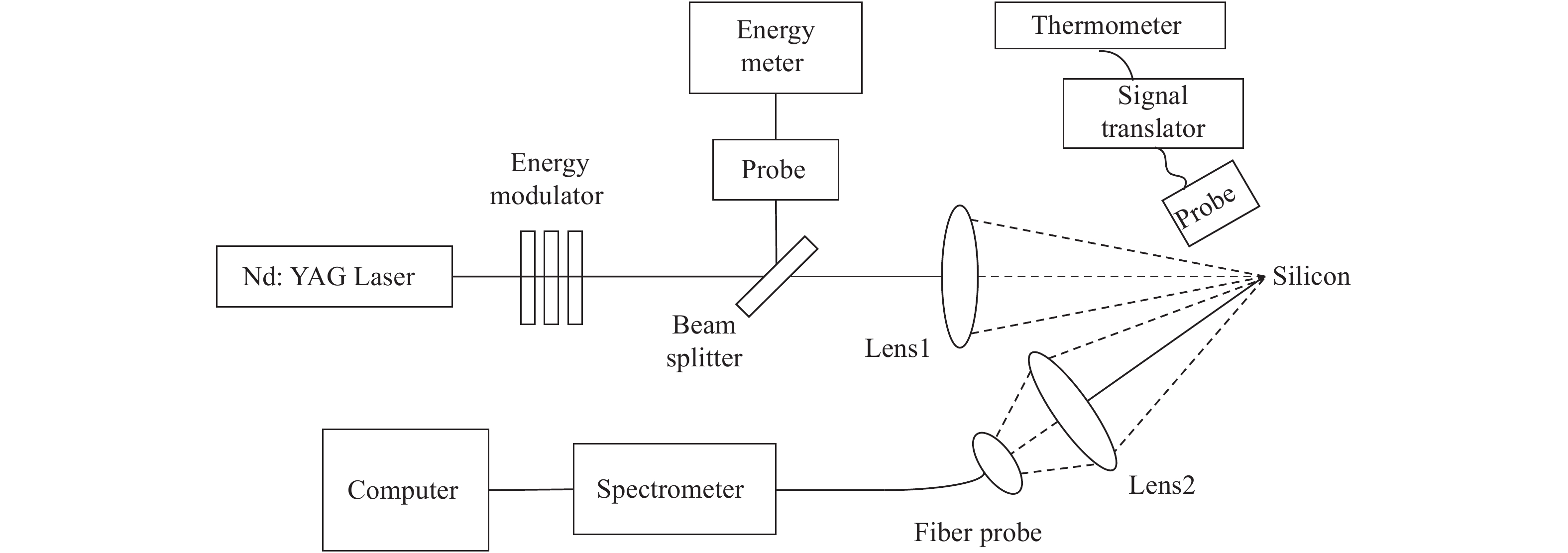
The experimental device for measuring the transient temperature of millisecond pulsed laser damage monocrystalline silicon is shown in Fig.1. The millisecond pulse laser used in the experiment is Melar-100Nd:YAG, it has a wavelength of 1 064 nm, the millisecond pulse width is adjustable from 1.0 to 3.0 ms, and the step size is 0.5 ms. The spatial distribution of the laser intensity is near Gaussian, and the laser is single pulse output. The exit beam diameter is about 2.0 cm. The laser is incident perpendicularly through the focusing lens (f’=300 mm). On the surface of the monocrystalline silicon sample, the spot diameter is 2.0 mm. Adjust the spot size by controlling the target position through a five-dimensional translation stage. The target is a single-sided polished monocrystalline silicon block with a crystal plane orientation of (100) type. The target is clamped on a five-dimensional translation stage. The surface temperature of the monocrystalline silicon was directly measured by high-precision spot thermometer. The high-precision measuring instrument adopts the German KMGA740 high-speed thermometer, the response time is 10 µs, and the accuracy is 0.75% of the measured value. Temperature measurement range is 623−3 773 K.
Figure 1.Experimental system for damage of monocrystalline silicon by long pulse laser
Due to the small test temperature range of the high-precision spot thermometer (623−3 773 K), significant saturation phenomenon occurs when it was irradiated by large-energy-density laser. At the same time, the laser-induced plasma generated radiation and caused interference over the point thermometer. Therefore, the spectral inversion method was utilized to invert the temperature of the process when the monocrystalline silicon was irradiated by high-energy solid pulsed laser. The QE6500 spectrometer was used to collect the spectrum during the laser action, and the spectral data in a specific area of the surface of the monocrystalline silicon was obtained, thereby the temperature of the region was inverted.
In multi-spectral temperature inversion system, Spectrometer model is QE6500 of American Ocean Optics. The measurement range is 200−1 100 nm, the quantum efficiency is up to 90%, and the resolution limit is 0.14 nm. The focal length of the condenser lens is 6 cm. the data curve is smoothed and fitted by measuring the spectrum-strength curve within certain integral time on the part of the monocrystalline silicon surface which is irradiated by laser. It provides a quantitative basis for the thermal damage law and mechanism research of the monocrystalline silicon which is acted by laser.
The spectral radiation emittance of the Planck formula is expressed as follows:
During the experiment of the laser interact with target, the spectrum curve of the 400-820 nm band was acquired by the spectrometer through the fiber optic probe, and the spectrum was displayed on the computer by SpectraSuite Setup software. The average of the laser surface area of the target surface was obtained by the Planck formula inversion temperature.
2 Results and analysis
2.1 Analysis of temperature characteristics of monocrystalline silicon
By experimental system of Fig.1, the relationship between the central point temperature on the monocrystalline silicon’s surface acted by different energy density lasers and time under single pulse condition is obtained, as is shown in Fig. 2.
Figure 2.Evolution of relationship between center temperature of monocrystalline silicon irradiated by lasers and time
It can be seen from Fig. 2 that: (1) The temperature of the laser irradiation center point gradually increases within the laser pulse width time, and the temperature rise curve deviates when the temperature reaches the melting point, the temperature rise rate decreases, and the penetration depth increases. When the monocrystalline silicon changes from solid to liquid, the reflectivity becomes larger (liquid reflection coefficient is 0.72,solid state reflection coefficient 0.33) and the energy it absorbs decreases (solid: 3.8×10³ m−1−3.7×10⁶ m−1, liquid: 8.6×10⁷ m−1). At the same time, some of the laser energy is converted into latent heat of phase change. As the laser energy density increases, the deflection degree of the temperature rise curve becomes smaller, which is mainly because of that the temperature rise speed is greater than the fallback speed; (2) When the temperature reaches the vicinity of the monocrystalline silicon’s vaporization point, the heat transfer coefficient of the high-temperature monocrystalline silicon becomes smaller, the heat transfer rate becomes slower, the laser energy transfer time becomes longer, and the vaporization plateau period appears; (3) When the time is longer than the pulse width time, the laser stops irradiating the monocrystalline silicon, and the monocrystalline silicon enters the thermal diffusion stage, and the temperature at the center point of the surface drops. When monocrystalline silicon undergoes liquid-solid phase transition (1 687 K), the falling speed is slow, and the solidification plateau occurs. When the monocrystalline silicon completes liquid crystal-solid phase change, the temperature will drop rapidly, and the laser energy density will increase. The more energy it absorbs, the longer the platform period becomes.
Figure 3 shows the variation laws of the center point temperature of the laser on the upper surface of the monocrystalline silicon with the changes of the energy density and pulse width. It can be seen from Fig. 3(a) that the peak point of the monocrystalline silicon laser action decreases with the increase of the pulse width, and the slope of the temperature rise curve increases with the increase of the pulse width. The peak temperature at the center point of monocrystalline silicon’s surface increases as the laser energy density increases. It can be seen from Fig. 3(b) that: (1)Under fixed pulse width, the temperature of the monocrystalline silicon increases with the increase of the laser energy density, and the temperature rises faster (2) for the fixed laser energy density, the temperature rise becomes slow when with the pulse width increases. Since the center point temperature at the surface of monocrystalline silicon is determined by the laser power density at this point, the larger the pulse width, the smaller the laser power density becomes, and the temperature at the center point of the monocrystalline silicon surface drops.
Figure 3.Relationship between the peak temperature of center point of monocrystalline silicon laser irradiation and the energy density and pulse width
Figure 4 is a graph showing the relationship between the temperature of the monocrystalline silicon laser irradiation center point and the changes with the energy density and the pulse width based on the spectral inversion method. Since the test integration time is longer than the laser action pulse width, the vaporization temperature of monocrystalline silicon is about 3 175 K, and the temperature measured by the experimental UV-visible spectrum is higher than 3 790 K. Since the test integration time is larger than the laser action pulse width, it can be considered as the highest temperature during the process of laser action.
Figure 4.Temperature variation and with energy density and pulse width
The temperature changes of laser damage monocrystalline silicon with the change of energy density and pulse width are approximately in equal-gradient distribution. The energy density is in the range of 1 800−2 500 J/cm2. With the increase of the energy density. The temperature of the monocrystalline silicon laser damage under the same pulse width is increasing. When the energy density is between 1 600 J/cm2and 1 800 J/cm2, the gradient of temperature changes with the change of the pulse width is small.
2.2 Analysis of damage structure of laser irradiated monocrystalline silicon
The damage morphology of monocrystalline silicon was measured through using an IF-0400 automatic zoom three-dimensional surface measuring instrument and a Leica DMI5000M metallographic microscope.
Figure 5 (a) shows the cleavage structure of monocrystalline silicon damaged by millisecond pulsed laser. The peak temperature of the laser irradiation center point is 1 417.5 K. Monocrystalline silicon is a brittle material with narrow plastic zone. When the thermal stress reaches the yield limit of monocrystalline silicon, brittle cracks will occur.
Figure 5.Cleavage damage structure of monocrystalline silicon
When monocrystalline silicon is irradiated by low energy density laser, the surface absorbs the irradiated laser energy and diffuses it into the body in the form of heat conduction. The temperature field formed inside the monocrystalline silicon is not even, and a large temperature gradient is formed. Thermal stress occurs in the monocrystalline silicon under the action of deformation mechanism. Fracture lines appear at the spot position. The cleavage cracks are mainly caused by the effect of thermal stress. Due to the anisotropy of monocrystalline silicon, it is a typical diamond structure in atomic arrangement, (111) cleavage fracture is most likely to occur on the crystal plane. In the experiment, the surface orientation of the monocrystalline silicon sample is (100) crystal plane orientation, (111) crystal plane group is 90°on (100) crystal plane, and vertical cracks are formed on (100) crystal plane when cleavage fracture occurs.
When the laser energy density reaches the melting threshold, the damage structure of monocrystalline silicon is shown in Fig. 5 (b). The peak temperature of the laser irradiation center point is 1 922.5 K. Some parts near the center of the spot melt. It can be seen from the graph that there is a cleavage zone on the surface of monocrystalline silicon target, and the cleavage crack has a rectangular structure.
The temperature of monocrystalline silicon increases after laser irradiation, and the shear failure strength of monocrystalline silicon decreases with the increase of temperature. Thermal stress occurs in monocrystalline silicon under the action of deformation mechanism, and cleavage cracks are mainly caused by thermal stress. The cleavage dislocation occurs along the cleavage plane of monocrystalline silicon and generates cleavage dislocation, which provides the starting point for brittle fracture of monocrystalline silicon target. Because the stress-induced dislocation region overlaps with the laser thermal damage region mostly, even if there are dislocations in the overlapping region, they will be eliminated by thermal melting. But there are cleavage dislocations outside the thermal damage region, cleavage damage is prior to thermal melting damage.
Figure 6 shows the multi-effect coupling damage morphology of monocrystalline silicon with pulse width of 1.5 ms and energy density of 95.5 J/cm2 laser. The peak temperature of laser irradiation center point is 2 535.9 K. According to the damage characteristics in the figure, the damage area can be divided into cleavage zone, melting zone, crack zone and splash zone.
It can be seen from Fig.6 that: (1) There is obvious melting phenomenon on the surface of monocrystalline silicon target, the ablation damage is aggravated and the ablation area is large. At the same time, there are granular substances on the surface of monocrystalline silicon, and droplet ejection occurs. The ejection of droplets is formed by phase explosion and explosive boiling, which conforms to the mechanism of droplet ejection in ablation theory. When monocrystalline silicon target is irradiated by millisecond pulsed laser, there are obvious ablation pits in the laser damage area due to the uneven distribution of laser field and the local differences of the target material. The size and depth of the pits are closely related to the distribution of the laser field and the inhomogeneity of the target material. When the monocrystalline silicon undergoes ignition damage, the plasma expansion produced during the damage process has a greater impact pressure on the monocrystalline silicon. So all the liquid substances produced during the laser action are sputtered out, and there are obvious splashing particles around it. (2) The absorption coefficient of monocrystalline silicon target increases with the increase of temperature in the solid phase region, and the temperature of the target increases faster. The cleavage dislocation produced by monocrystalline silicon target provides the starting point for brittle fracture. When the laser stops irradiating the monocrystalline silicon target, the stress perpendicular to the cleavage surface is tensile stress, and the stress will concentrate on the dislocation defect. So brittle cracks can be observed at the edge of the laser thermal damage area. At the same time, the dislocation lines in the surface melting area become sparse due to the destruction of the crystal structure of monocrystalline silicon by thermal melting.
Figure 6.Metallographic structure of multi-effect coupling damage in monocrystalline silicon
Figure 7 shows the morphology of the monocrystalline silicon target with energy density of 318.5 J/cm2. As can be seen from the figure, when the monocrystalline silicon produces ignition damage, the ablation area becomes larger. Thermal diffusion and subsequent boiling will cause the increase of the depth of the corrosion pit. In the process of ablation pit formation and stabilization, the Margrani effect has only a weak effect compared with the back stamping force and surface tension. The stress zone and the splashing zone are mixed together, and the damage area is gradually increasing. Laser energy mainly concentrates on the bottom of the ablation pit. There is a great back-pressing force at the bottom of the pit. The gas dynamic effect leads to a strong back-flow. The back-pressing force causes the upward flow of the fluid. In the early stage of the formation of the ablation pit, the molten fluid can easily be pushed upward to the pit due to the back-pressing effect. With the increase of the depth of the pit, even the high back-pressing force is applied to the ablation pit, especially at the bottom of the pit, it is not enough to push all the molten fluid out of the pit, as viscous shear stress weakens the momentum of upward flow of the fluid; while the surface tension formed by the hydrodynamic pressure and uneven temperature field causes the downward flow of the ablation pit fluid. The convex flow and collision result in the "spike" structure in the pit.
Figure 7.Peak corrosion damage structure of monocrystalline silicon
Figure 8 shows the relationship between the ablation depth of monocrystalline silicon and the laser energy density under the condition of 1.0 ms pulse width and single pulse laser. It can be seen from the figure that the laser ablation depth increases with the increase of laser energy density under the condition of fixed pulse width; when the laser energy density is less than 200 J/cm2, the damage depth of monocrystalline silicon does not change much, and maintains near 100 μm, and when the laser energy density is more than 200 J/cm2, the damage depth of monocrystalline silicon increases rapidly with the increase of laser energy density.
Figure 8.Relationships between damage depth and laser energy density
Figure 9 shows the relationship between the etching depth of monocrystalline silicon and the number of pulses under the condition of pulse train laser with the pulse width of 1.0 ms, the spot diameter is 4.0 mm, and the laser energy density of 266.7 J/cm2. It can be seen from the figure that the corrosion depth increases with the increase of the number of pulses. When the number of pulses is larger than 30, the corrosion depth increases sharply.
Figure 9.Relationship between the etching depth of monocrystalline silicon and number of pulse
In this paper, the monocrystalline silicon is irradiated with millisecond pulsed laser to analyze the temperature evolution and damage structure of the monocrystalline silicon during thermal damage. Under the action of millisecond laser, the peak temperature of monocrystalline silicon increases with the increase of energy density, and decreases with the increase of pulse width. The temperature rise curve shows a deflection near the melting point, mainly due to the phase transition of monocrystalline silicon from solid to liquid. Latent heat, the reflectivity becomes larger, and as the energy density increases, the deflection becomes smaller due to the increase of the temperature rise rate; when the higher energy density laser acts, the gasification plateau occurs, and after the pulse action stops, the solidification platform appears due to the release of the latent heat temperature. When the laser irradiation center point temperature reaches 1 417.5 K, a clear cleavage structure appears, and the cleavage crack is a rectangular structure. When the peak temperature is 1 922.5 K, the corrosion occurs, the thermal ablation removes the cleavage, and there are still cleavage dislocations outside the heat damage zone, and the thermal cleavage damage precedes the thermal induced corrosion damage. When the peak temperature is 2 535.9 K, the monocrystalline silicon has multi-effect coupling damage; when the laser energy density is less than 200 J/cm2, the damage depth is about 100μm, the damage depth increases with the increase of energy density, and increases rapidly with the increase of pulse number. This study provides a reference for laser fine processing, and provides a scientific basis for the design of high-precision laser weapons and the improvement of laser hardening measures of monocrystalline silicon.
[7] L Zhang, X Ni, J Lu. Numerical simulation of vaporization effect of long pulsed laser interaction with silicon. Optics and Precision Engineering, 19, 11-19(2011).
[8] Z Li, H Zhang, Z Shen. Time-resolved temperature measurement and numerical simulation of millisecond laser irradiated silicon. Journal of Applied Physics, 114, H39-H41(2013).
[9] C B Zhang, J D Zhang, H G Wang. Damage characteristic of microwave pulse injected on Si bipolar transistor. Journal of National University of Defense Technology, 1-4(2015).
[10] Y X Cui, X Y Nu, C L Wang. Numerical analysis of CW laser damage in Germanium. Journal of Applied Optics, 19, 267-271(2011).
Ming Guo, Yongxiang Zhang, Wenying Zhang, Hong Li. Thermal damage of monocrystalline silicon irradiated by long pulse laser[J]. Infrared and Laser Engineering, 2020, 49(3): 0305002