• Photonics Research
  • Vol. 6, Issue 1, 24 (2018)
Huifang Zhang1, Xueqian Zhang1、*, Quan Xu1, Qiu Wang1, Yuehong Xu1, Minggui Wei1, Yanfeng Li1, Jianqiang Gu1, Zhen Tian1, Chunmei Ouyang1, Xixiang Zhang2, Cong Hu3, Jiaguang Han1、5, and Weili Zhang1、4、6
Author Affiliations
  • 1Center for Terahertz waves and College of Precision Instrument and Optoelectronics Engineering, Tianjin University and the Key Laboratory of Optoelectronics Information and Technology (Ministry of Education), Tianjin 300072, China
  • 2Physical Science and Engineering Division, King Abdullah University of Science and Technology, Thuwal 23955-6900, Saudi Arabia
  • 3Guangxi Key Laboratory of Automatic Detecting Technology and Instruments, Guilin University of Electronic Technology, Guilin 541004, China
  • 4School of Electrical and Computer Engineering, Oklahoma State University, Stillwater, Oklahoma 74078, USA
  • 5e-mail: jiaghan@tju.edu.cn
  • 6e-mail: weili.zhang@okstate.edu
  • show less
    DOI: 10.1364/PRJ.6.000024 Cite this Article Set citation alerts
    Huifang Zhang, Xueqian Zhang, Quan Xu, Qiu Wang, Yuehong Xu, Minggui Wei, Yanfeng Li, Jianqiang Gu, Zhen Tian, Chunmei Ouyang, Xixiang Zhang, Cong Hu, Jiaguang Han, Weili Zhang. Polarization-independent all-silicon dielectric metasurfaces in the terahertz regime[J]. Photonics Research, 2018, 6(1): 24 Copy Citation Text show less
    Schematic of the silicon pillar structure and the simulated results of the selected eight silicon pillars. (a) Schematic of a silicon pillar in the uniform hexagonal lattice on a silicon substrate. The lattice constant p=100 μm, and the pillar height h=150 μm. (b) Simulated phase shifts and transmission amplitudes of the eight selected silicon pillars with different diameters d at 1.0 THz. The diameters corresponding to the pillars in the upper row from number 1–8 are d=20, 44.5, 53.5, 60, 66.5, 73, 79.5, and 88.5 μm, respectively. (c) Simulated side views (x–z planes) of the magnetic energy density distributions in four silicon pillars among the eight selections with d=44.5, 60, 73, and 88.5 μm, respectively, at 1.0 THz. An x-polarized plane wave with magnetic energy density of 1 is normally incident on the silicon pillars from the bottom (substrate side).
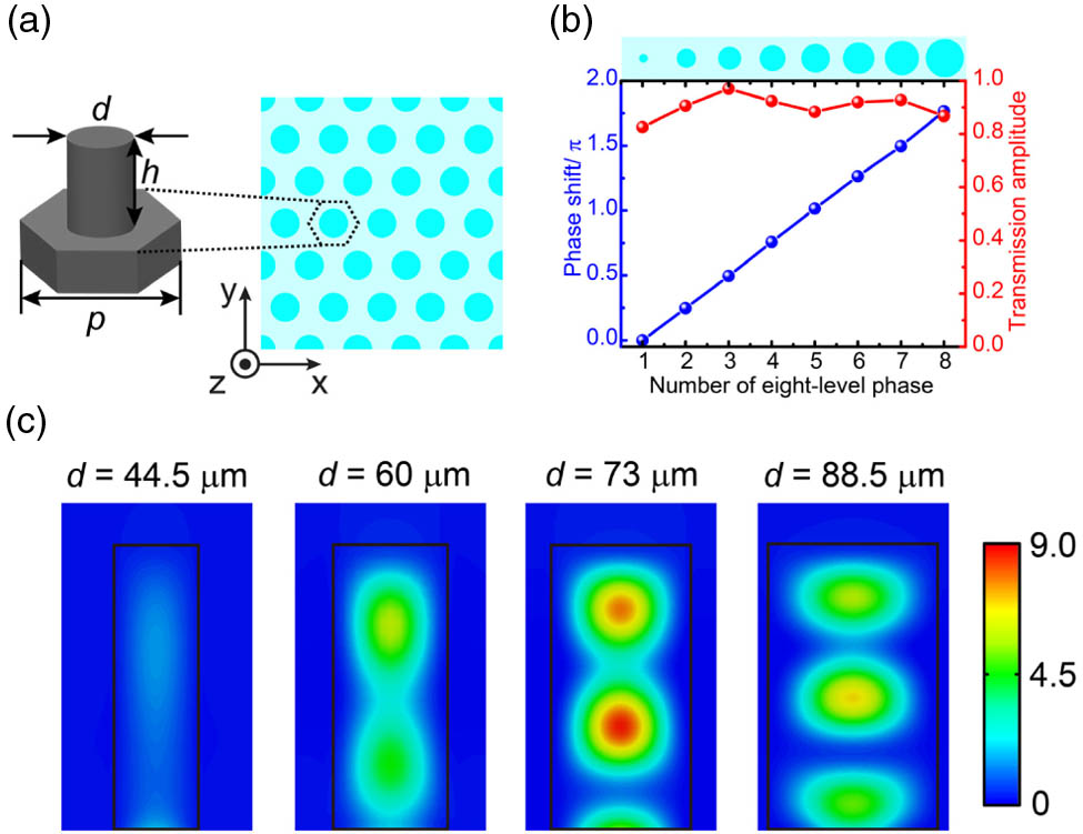
    Fig. 1. Schematic of the silicon pillar structure and the simulated results of the selected eight silicon pillars. (a) Schematic of a silicon pillar in the uniform hexagonal lattice on a silicon substrate. The lattice constant p=100  μm, and the pillar height h=150  μm. (b) Simulated phase shifts and transmission amplitudes of the eight selected silicon pillars with different diameters d at 1.0 THz. The diameters corresponding to the pillars in the upper row from number 1–8 are d=20, 44.5, 53.5, 60, 66.5, 73, 79.5, and 88.5 μm, respectively. (c) Simulated side views (xz planes) of the magnetic energy density distributions in four silicon pillars among the eight selections with d=44.5, 60, 73, and 88.5 μm, respectively, at 1.0 THz. An x-polarized plane wave with magnetic energy density of 1 is normally incident on the silicon pillars from the bottom (substrate side).
    SEM image and experimental results of the anomalous deflector. (a) SEM image of part of the anomalous deflector. Scale bar: 200 μm, same hereinafter. (b) Schematic of FAT TDS. (c) Measured normalized far-field intensity distribution as a function of the deflection angle θ and the frequency under normal incidence. (d) Corresponding far-field intensity profile at 1.0 THz extracted from (c).
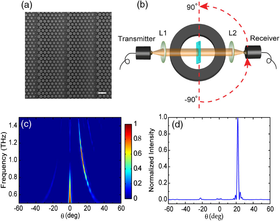
    Fig. 2. SEM image and experimental results of the anomalous deflector. (a) SEM image of part of the anomalous deflector. Scale bar: 200 μm, same hereinafter. (b) Schematic of FAT TDS. (c) Measured normalized far-field intensity distribution as a function of the deflection angle θ and the frequency under normal incidence. (d) Corresponding far-field intensity profile at 1.0 THz extracted from (c).
    SEM image of the B0 generator and experimental results of the B0, B1, and B2 generators. (a) SEM image of part of the fabricated B0 generator. (b) Schematic of FNSTM. (c, f, i) Measured normalized intensity distributions of the B0, B1, and B2 generators in the x–z planes, respectively, at 1.0 THz. (d, g, j) The corresponding measured normalized intensity distributions in the x–y planes. (e, h, k) The corresponding measured phase distributions in the x–y planes. The intensity and phase distributions in the x–y planes of the B0, B1, and B2 generators are detected at 5, 5, and 6 mm away from the generators, respectively. The scanning step is 0.25 mm.
    Fig. 3. SEM image of the B0 generator and experimental results of the B0, B1, and B2 generators. (a) SEM image of part of the fabricated B0 generator. (b) Schematic of FNSTM. (c, f, i) Measured normalized intensity distributions of the B0, B1, and B2 generators in the xz planes, respectively, at 1.0 THz. (d, g, j) The corresponding measured normalized intensity distributions in the xy planes. (e, h, k) The corresponding measured phase distributions in the xy planes. The intensity and phase distributions in the xy planes of the B0, B1, and B2 generators are detected at 5, 5, and 6 mm away from the generators, respectively. The scanning step is 0.25 mm.
    SEM images and experimental results of the V1, V2, and V4 generators. (a, d, g) SEM images of part of the fabricated V1, V2, and V4 generators, respectively. The different color shades represent different phase sections schematically, as indicated by (a). (b, e, h) Measured phase distributions of the output electric fields of the V1, V2, and V4 generators, respectively, at 1.0 THz. (c, f, i) The corresponding measured normalized intensity distributions. All of the distributions are detected at a distance of 10 mm from the generators. The scanning step is 0.4 mm.
    Fig. 4. SEM images and experimental results of the V1, V2, and V4 generators. (a, d, g) SEM images of part of the fabricated V1, V2, and V4 generators, respectively. The different color shades represent different phase sections schematically, as indicated by (a). (b, e, h) Measured phase distributions of the output electric fields of the V1, V2, and V4 generators, respectively, at 1.0 THz. (c, f, i) The corresponding measured normalized intensity distributions. All of the distributions are detected at a distance of 10 mm from the generators. The scanning step is 0.4 mm.
    Schematic of the CB1 generator and the corresponding experimental results. (a) Schematic of the CB1 composite beam generator composed of the V1 and B0 generators. The terahertz beam is incident from the V1 generator. (b) Measured normalized intensity distributions of the CB1 generator in the x–z plane at 1.0 THz. (c, d) The corresponding measured normalized intensity and phase distributions in the x–y plane, respectively. The intensity and phase distributions in the x–y plane are detected at 5 mm away from the generator. The scanning step is 0.25 mm.
    Fig. 5. Schematic of the CB1 generator and the corresponding experimental results. (a) Schematic of the CB1 composite beam generator composed of the V1 and B0 generators. The terahertz beam is incident from the V1 generator. (b) Measured normalized intensity distributions of the CB1 generator in the xz plane at 1.0 THz. (c, d) The corresponding measured normalized intensity and phase distributions in the xy plane, respectively. The intensity and phase distributions in the xy plane are detected at 5 mm away from the generator. The scanning step is 0.25 mm.
    Huifang Zhang, Xueqian Zhang, Quan Xu, Qiu Wang, Yuehong Xu, Minggui Wei, Yanfeng Li, Jianqiang Gu, Zhen Tian, Chunmei Ouyang, Xixiang Zhang, Cong Hu, Jiaguang Han, Weili Zhang. Polarization-independent all-silicon dielectric metasurfaces in the terahertz regime[J]. Photonics Research, 2018, 6(1): 24
    Download Citation