Mengxia Wang1、2、3, Hailong Qiu3、8、*, Tianwen Yang3, Zhengping Wang4, Chuanrui Zhao4, Yuanan Zhao1、2、9、*, Ting Yu5, Yuyao Jiang5、6, Meiling Chen1、2, Yafei Lian1、2, Ge Zhang1、2, Hongjun Liu3, Zhanggui Hu3, and Jianda Shao1、2、7、10、*
Author Affiliations
1Laboratory of Thin Film Optics, Shanghai Institute of Optics and Fine Mechanics, Chinese Academy of Sciences, Shanghai 201800, China2Center of Materials Science and Optoelectronics Engineering, University of Chinese Academy of Sciences, Beijing 100049, China3Tianjin Key Laboratory of Functional Crystal Materials, Institute of Functional Crystal, Tianjin University of Technology, Tianjin 300384, China4State Key Laboratory of Crystal Materials, Shandong University, Jinan 250100, China5Laboratory of High Power Fiber Laser Technology, Shanghai Institute of Optics and Fine Mechanics, Chinese Academy of Sciences, Shanghai 201800, China6College of Science, Shanghai University, Shanghai 200444, China7Hangzhou Institute for Advanced Study, University of Chinese Academy of Sciences, Hangzhou 310024, China8e-mail: qiu@tjut.edu.cn9e-mail: yazhao@siom.ac.cn10e-mail: jdshao@siom.ac.cnshow less
DOI: 10.1364/PRJ.461522
Cite this Article
Set citation alerts
Mengxia Wang, Hailong Qiu, Tianwen Yang, Zhengping Wang, Chuanrui Zhao, Yuanan Zhao, Ting Yu, Yuyao Jiang, Meiling Chen, Yafei Lian, Ge Zhang, Hongjun Liu, Zhanggui Hu, Jianda Shao. Broadband 1T-polytype tantalum disulfide saturable absorber for solid-state bulk lasers[J]. Photonics Research, 2022, 10(9): 2122
Copy Citation Text
show less
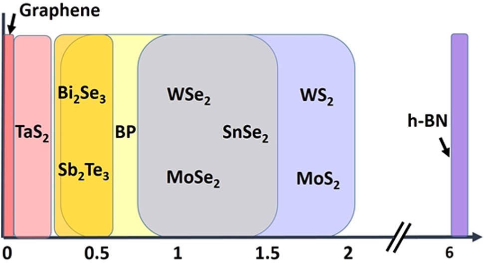
Fig. 1. Band gap distribution of several typical 2D materials.
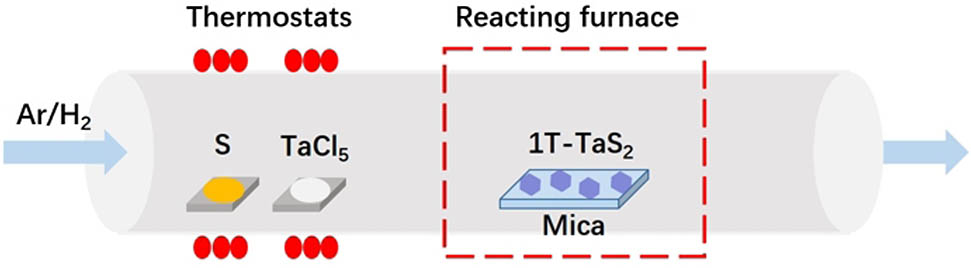
Fig. 2. Schematic diagram of CVD reactor.
Fig. 3. (a) Crystal structure of 1T-TaS2. (b) XRD pattern of the 1T-TaS2. (c) Typical SEM image of 1T-TaS2 nanosheets on mica substrate. (d) AFM image of the 1T-TaS2 nanosheets and the typical height profile. (e) Selected area electron diffraction of 1T-TaS2 nanosheets. (f) High-resolution TEM image of 1T-TaS2 nanosheets.
Fig. 4. (a) Visible NIR transmission spectra of the 1T-TaS2 sample and mica substrate in the range 0.2–2.5 μm. (b) FTIR transmission spectrum in the range 1.5–10 μm.
Fig. 5. (a) TAS pumped at 1500 nm and probed from 490 to 900 nm. (b) TAS pumped at 1500 nm and probed from 700 to 1100 nm. (c), (d) Extracted TAS with different delay time.
Fig. 6. (a) Attenuation dynamic curve at different wavelengths. (b) Illustration of the carrier dynamics process in 1T-TaS2.
Fig. 7. (a) Schematic of saturable absorption. Z-scan results of 1T-TaS2 sample at (b) 515 nm, (c) 1030 nm, (d) 1500 nm, (e) 2000 nm, and (f) 2500 nm. Insets show the variations in the transmittance with incident intensity.
Fig. 8. Passively Q-switched laser performance of the 1T-TaS2. Pulse width and repetition frequency, single-pulse energy and peak power, the corresponding pulse trains and single-pulse profiles at (a)–(c) 1.06 μm, (d)–(f) 1.34 μm, and (g)–(i) 1.94 μm.
(nm) | (ps) | (ns) | (ns) |
---|
726 | 0.35 | 0.11 | 6.50 | 973 | 0.46 | 0.19 | 7.56 | 1030 | 0.57 | 0.18 | 8.78 |
|
Table 1. Fitting Parameters of TAS Dynamics of 1T-TaS2 at Different Wavelengths
Material | (nm) | () | (%) | () | Reference |
---|
| 515 | | 15.4 | 1.2 | This work | 1030 | | 6.7 | 0.2 | 1500 | | 9.4 | 6.4 | 2000 | | 9.6 | 27.4 | 2500 | | 6.6 | 28.8 | Graphene | 515 | −10.5 | — | 2.6 | [61] | 1030 | −12.4 | — | 3.2 | BP | 532 | | — | — | [62] | 1060 | | 15.6 | | [63] | | 1030 | | — | — | [64] | | 1040 | | — | — | [65] | | 1030 | −0.96 | — | — | [66] | Te/PVP | 1060 | | 10.5 | | [60] |
|
Table 2. NLO Parameters of 1T-TaS2 and Other Typical 2D SA Materials
(μm) | Laser Crystal | Laser Properties |
---|
Absorbed Pump Power (W) | CW Output Power (W) | Q-switched Output Power (mW) | Pulse Width (ns) | Single-pulse Energy (μJ) | Peak Power (W) |
---|
1.06 | Nd:YAG | 1.10 | 0.38 | 102 | 200 | 0.48 | 2.41 | 1.34 | | 2.03 | 0.75 | 85 | 110.5 | 0.21 | 1.87 | 1.94 | Tm:YAP | 4.11 | 1.37 | 323 | 692.5 | 3.89 | 5.62 |
|
Table 3. Passive Q-switching Performance for a Solid-State Laser of 2D 1T-TaS2