• Photonics Research
  • Vol. 10, Issue 9, 2122 (2022)
Mengxia Wang1、2、3, Hailong Qiu3、8、*, Tianwen Yang3, Zhengping Wang4, Chuanrui Zhao4, Yuanan Zhao1、2、9、*, Ting Yu5, Yuyao Jiang5、6, Meiling Chen1、2, Yafei Lian1、2, Ge Zhang1、2, Hongjun Liu3, Zhanggui Hu3, and Jianda Shao1、2、7、10、*
Author Affiliations
  • 1Laboratory of Thin Film Optics, Shanghai Institute of Optics and Fine Mechanics, Chinese Academy of Sciences, Shanghai 201800, China
  • 2Center of Materials Science and Optoelectronics Engineering, University of Chinese Academy of Sciences, Beijing 100049, China
  • 3Tianjin Key Laboratory of Functional Crystal Materials, Institute of Functional Crystal, Tianjin University of Technology, Tianjin 300384, China
  • 4State Key Laboratory of Crystal Materials, Shandong University, Jinan 250100, China
  • 5Laboratory of High Power Fiber Laser Technology, Shanghai Institute of Optics and Fine Mechanics, Chinese Academy of Sciences, Shanghai 201800, China
  • 6College of Science, Shanghai University, Shanghai 200444, China
  • 7Hangzhou Institute for Advanced Study, University of Chinese Academy of Sciences, Hangzhou 310024, China
  • 8e-mail: qiu@tjut.edu.cn
  • 9e-mail: yazhao@siom.ac.cn
  • 10e-mail: jdshao@siom.ac.cn
  • show less
    DOI: 10.1364/PRJ.461522 Cite this Article Set citation alerts
    Mengxia Wang, Hailong Qiu, Tianwen Yang, Zhengping Wang, Chuanrui Zhao, Yuanan Zhao, Ting Yu, Yuyao Jiang, Meiling Chen, Yafei Lian, Ge Zhang, Hongjun Liu, Zhanggui Hu, Jianda Shao. Broadband 1T-polytype tantalum disulfide saturable absorber for solid-state bulk lasers[J]. Photonics Research, 2022, 10(9): 2122 Copy Citation Text show less

    Abstract

    1T-polytype tantalum disulfide (1T-TaS2), an emerging strongly correlated material, features a narrow bandgap of 0.2 eV, bridging the gap between zero-bandgap graphene and large-bandgap 2D nonlinear optical (NLO) materials. Combined with its intense light absorption, high carrier concentration, and high mobility, 1T-TaS2 shows considerable potential for applications in broadband optoelectronic devices. However, its NLO characteristics and related applications have rarely been explored. Here, 1T-TaS2 nanosheets are prepared by chemical vapor deposition. The ultrafast carrier dynamics in the 400–1100 nm range and broadband NLO performance in the 515–2500 nm range are systematically studied using femtosecond lasers. An obvious saturable absorption phenomenon is observed in the visible to IR range. The nonlinear absorption coefficient is measured to be -22.60±0.52 cm MW-1 under 1030 nm, which is larger than that of other typical 2D saturable absorber (SA) materials (graphene, black phosphorus, and MoS2) under similar experimental conditions. Based on these findings, using 1T-TaS2 as a new SA, passively Q-switched laser operations are successfully performed at 1.06, 1.34, and 1.94 μm. The results highlight the promise of 1T-TaS2 for broadband optical modulators and provide a potential candidate material system for mid-IR nonlinear optical applications.

    1. INTRODUCTION

    Pulsed lasers have attracted tremendous interest owing to their excellent time-domain and frequency-domain characteristics. They have been applied in various applications, such as industrial processing, atmospheric monitoring, medical surgery, and scientific research [13]. The passive modulation technique is a standard method to obtain a pulsed laser, which has the advantages of low cost, simple structure, and easy implementation [4]. The critical component, the saturable absorber (SA), is synthesized based on the saturable absorption characteristics of nonlinear optical (NLO) materials. With the development of pulsed lasers for high power, short pulses, tunable operating wavelengths, and miniaturization, the demand for NLO materials with excellent comprehensive wideband performance has become more apparent [5,6].

    The ideal NLO materials for SAs should have the characteristics of large nonlinearity, a wide absorption band, a fast response time, ambient atmospheric stability, high-power processing capacity, low optical loss, and low cost [7,8]. Traditional chromium-doped yttrium aluminum garnet crystals and semiconductor saturable absorber mirrors have several drawbacks that seriously limit their practical applications, especially in the mid-IR (MIR) band: narrowband operation, wavelength sensitivity, limited response time, and complex preparation processes [911].

    In recent years, 2D materials have attracted tremendous interest because of their unique electronic and optical properties, including adjustable bandgap values and band structures, high carrier density and mobility, and ultrawide NLO responses [1216]. Combined with their mechanical flexibility and good compatibility with optical elements, various 2D materials such as graphene, black phosphorus (BP), transition metal dichalcogenides (TMDs), and topological insulators (TIs) have been practically applied in photoelectric devices [1722]. Among them, TMDs have the chemical formula MX2 (M=Mo, W, Re, and X=S, Se, Te, for example) and display a “sandwich” stacking that is formed by the sequential stacking of X–M–X planes. Adjacent sandwich structures are bonded by weak van der Waals forces, providing the potential for stripping bulk TMDs into a few layers. Owing to quantum confinement and surface effects, most 2D TMDs exhibit stronger light–matter interactions and NLO responses than bulk materials [23,24]. Compared to 2D materials composed of single elements, TMDs have more abundant component elements and diversified electronic structures, thus having unique physical and chemical properties. Depending on the different coordination modes of the transition metal atoms, TMDs exhibit various structural phases (1T, 2H, and 3R) and may behave as metallic, semiconducting, superconducting, or insulating. In addition, the optical and electronic characteristics of many TMD flakes are highly dependent on the number of layers and exhibit layer-dependent bandgaps [25]. Several demonstrations have shown that 2D TMDs possess excellent NLO characteristics, which can be used to fabricate SAs and realize the generation of pulsed lasers, primarily focusing on 2H-polytype TMDs [26,27]. However, owing to their intrinsic energy bandgap of 1–2 eV, 2H-polytype TMD has limitations in practical applications, especially for MIR optical modulators [28].

    Compared to 2H-polytype TMDs, research on the NLO properties and related applications of 1T-polytype TMDs is relatively sparse. As a 1T-polytype TMD, 1T-TaS2 has attracted significant attention in condensed matter physics and holds great potential for electronic and optoelectronic applications because of its low-dimensional, strongly correlated electron system and robust Coulomb interactions among internal electrons [2931]. The light–matter interaction in 1T-TaS2 is interesting because light can significantly alter the free energy landscape of strong correlations, resulting in many new physical phenomena [32,33], such as metal-to-insulator transitions, superconductivity, charge density waves, and others [3436]. In addition, 1T-TaS2 at ambient pressure exhibits metal-like characteristics with the band derived from the extra valence electrons of Ta across the Fermi level [37]. It is noteworthy that 1T-TaS2 features a narrow bandgap of 0.2 eV [38], bridging the gap between zero-bandgap graphene and large-bandgap 2D materials [BP, TIs, 2H-polytype TMDs, and boron nitride (h-BN)], as shown in Fig. 1, and has great potential for applications in broadband photonic and optoelectronic devices, especially in the MIR band. Meanwhile, 1T-TaS2 exhibits strong light absorption, ultrafast relaxation, high carrier concentration, and high mobility [39,40]. These remarkable properties make 1T-TaS2 a promising material, not only for fundamental physics research, but also for applications in ultrafast photonics. Therefore, it is of great significance to study the nonlinear absorption performance of 1T-TaS2 and explore its application in optoelectronic devices.

    Band gap distribution of several typical 2D materials.

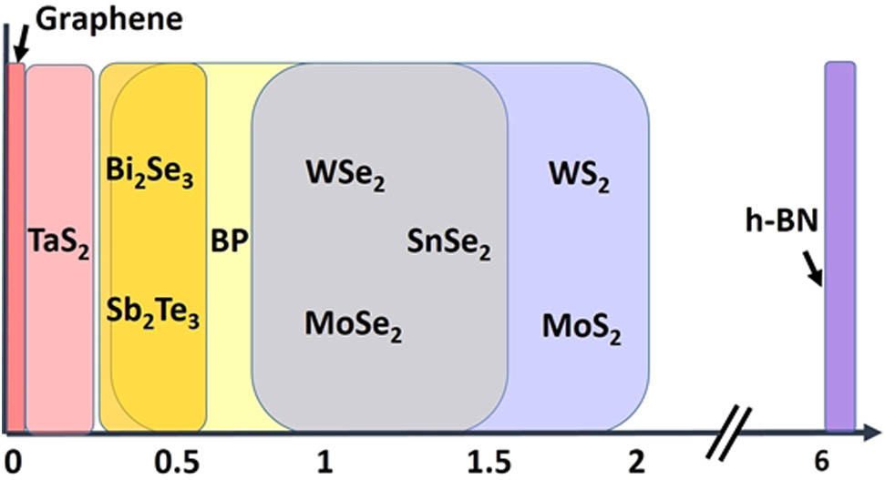
    Figure 1.Band gap distribution of several typical 2D materials.

    To date, 1T-TaS2 has been produced using various methods, including mechanical exfoliation, chemical vapor deposition (CVD), chemical vapor transport (CVT), and molecular beam epitaxy (MBE) [41,42]. Among them, the samples synthesized by the CVD method have high purity and good crystallization performance, which is of great importance to property investigation and device applications. However, the synthesis of samples with controllable thicknesses remains challenging. In this study, we used an improved CVD method to control the thickness of a 1T-TaS2 sample on a mica substrate. The sample exhibited a broad transparent region (0.2–8.7 μm). The transient absorption spectrum (TAS) demonstrated that 1T-TaS2 has an apparent ground-state bleaching phenomenon at all test wavelengths. In addition, we verified the NLO response of 1T-TaS2 in the range 0.5–2.5 μm with open aperture (OA) Z-scan experiments, and the sample exhibited a broadband saturable absorption phenomenon. Furthermore, to verify the potential of 1T-TaS2 as an SA, passively Q-switched laser operations were performed at 1–2 μm. These results demonstrate that 1T-TaS2 possesses excellent broadband nonlinear absorption properties and is a promising SA for pulsed lasers in the visible to MIR range. Strongly correlated materials, represented by 1T-TaS2, provide a unique material system for optoelectronic materials. While driving the continuing development of strongly correlated materials, it is expected to provide new laser modulators with excellent performance for ultrafast pulsed lasers.

    2. CRYSTAL GROWTH AND CHARACTERIZATION

    In this study, we used an improved atmospheric pressure CVD method to prepare 1T-TaS2. The schematic diagram of the CVD reactor is shown in Fig. 2. Because of small lattice mismatch with that of 1T-TaS2, excellent corrosion resistance, and easy stripping preparation process, the mica substrate with a smooth atomic surface was selected as the substrate and placed in the deposition area. Quantitative sulfur powder (purity higher than 99.9%) and TaCl5 powder (purity higher than 99.9%) were placed separately outside the furnace. For the source area, two thermostats are placed outside to heat the powder. After heating and gasification, the precursors were transmitted and mixed in the reactor to form 1T-TaS2 under the Ar/H2 (5%  H2, 100 sccm; sccm, standard cubic centimeters per minute) mixed carrier gas. The reaction equation involved in the preparation process is expressed as TaCl5(g)+H2(g)+S(g)TaS2(s)+HCl(g).

    Schematic diagram of CVD reactor.

    Figure 2.Schematic diagram of CVD reactor.

    During the reaction, the temperature inside the reactor was maintained at 850°C. TaCl5 was the key reactant that determined the reaction process. When the supply of the TaCl5 was stopped, the growth of the 1T-TaS2 stopped. Excess gaseous sulfur was discharged from the reactor, which did not affect the growth of the 1T-TaS2, but provided a reducing atmosphere to prevent the oxidation of the 1T-TaS2. With the continuous supply of S and intermittent supply of the TaCl5, the 1T-TaS2 with a controllable thickness and high crystalline quality was obtained. The crystal structure of 1T-TaS2 belongs to the hexagonal system (space group P3m1, a=b=3.36 Å, and c=5.90 Å) [43], which is composed of S–Ta–S atomic layers to form a similar “sandwich” structure, as shown in Fig. 3(a). The top three S atoms are centrally symmetric with the bottom three S atoms around the Ta atom in the center, forming an octahedral coordination of the 1T structure. The S–Ta–S planes form a layered structure following the stacking method of AA [44].

    (a) Crystal structure of 1T-TaS2. (b) XRD pattern of the 1T-TaS2. (c) Typical SEM image of 1T-TaS2 nanosheets on mica substrate. (d) AFM image of the 1T-TaS2 nanosheets and the typical height profile. (e) Selected area electron diffraction of 1T-TaS2 nanosheets. (f) High-resolution TEM image of 1T-TaS2 nanosheets.

    Figure 3.(a) Crystal structure of 1T-TaS2. (b) XRD pattern of the 1T-TaS2. (c) Typical SEM image of 1T-TaS2 nanosheets on mica substrate. (d) AFM image of the 1T-TaS2 nanosheets and the typical height profile. (e) Selected area electron diffraction of 1T-TaS2 nanosheets. (f) High-resolution TEM image of 1T-TaS2 nanosheets.

    X-ray diffraction (XRD) was used to characterize the crystallographic structure of the prepared 1T-TaS2 sample (Empyrean, Malvern Panalytical). Figure 3(b) shows typical XRD profiles of 1T-TaS2 nanosheets on a mica substrate, and the primary diffraction peaks matched well with those of the 1T-polytype TaS2 (No. 88-1008, Joint Commission on Powder Diffraction Standards). The XRD patterns showed sharp diffraction peaks, indicating a highly crystalline structure of the prepared 2D 1T-TaS2 nanosheets. The strong, sharp diffraction peak (001) at 14.6° shows the preferred orientation of a 1T-TaS2 crystal is (001) plane that is perpendicular to axis c. It represents the distance between adjacent layers in the 1T structure [45]. Additional diffraction peaks originating from the (100), (011), (102), (110), (103), (200), (201), (014), (022), and (113) planes were centered at 31.3°, 34.3°, 43.7°, 54.5°, 55.8°, 64.0°, 65.6°, 71.6°, 72.8°, and 74.1°, respectively. In addition, some weak peaks at 28.1°, 29.4°, 57.3°, and 67.9° were ascribed to trace amounts of Ta2O5 produced after a long period of time in an air environment (2 months). Based on the XRD profiles, we concluded that the prepared 2D TaS2 must have a 1T-polytype structure.

    To explore the surface morphology of the prepared 2D nanosheets, field-emission scanning electron microscopy (FESEM; Auriga, Carl Zeiss; WD: 7.8 mm; EHT: 1.50 kV; scan mode: SE2) was performed. As shown in Fig. 3(c), typical 1T-TaS2 nanosheets possess a regular hexagonal shape with a domain size of a few micrometers and are uniformly distributed on the mica substrate. To further analyze the surface topography and thickness information of the 1T-TaS2 nanosheets, atomic force microscopy (AFM; Dimension-3100, Veeco) was conducted. Figure 3(d) shows the AFM results of the 1T-TaS2 nanosheets in a 15  μm×15  μm area (inset) and the corresponding thickness. The average thickness is 18.7  nm, indicating that the number of layers of the prepared 1T-TaS2 nanosheets is approximately 29 (interlayer distance is 0.65  nm) [46].

    Transmission electron microscopy (TEM; Talos F200X, Thermo Fisher Scientific) was used to explore the structural arrangement of the prepared 1T-TaS2. The 2D nanosheets were transferred onto a copper grid prior to the TEM analysis. Figure 3(e) shows the selected area electron diffraction (SAED) pattern of the sample, where a set of points formed a six-fold rotational symmetry, indicating a well-defined periodic lattice and good crystallinity of the prepared 1T-TaS2 crystal. By analyzing the reciprocal lattice of 3.42  nm1, the direction of the zone axis was determined to be [001], which corresponds to the crystal planes of (100), (010), and (110). A high-resolution TEM (HRTEM) image of the 1T-TaS2 crystal is shown in Fig. 3(f). The interplanar distance along the three directions is the same (d=0.29  nm), corresponding to the three planes perpendicular to the [001] direction. The characterizations above confirm that the fabricated 2D nanosheets are 1T-polytype TaS2 nanosheets. The high crystal quality of 2D 1T-TaS2 provides a good foundation for subsequent optical testing and applications.

    To confirm the linear optical properties of the prepared 1T-TaS2 sample, the transmission spectrum was measured with a PerkinElmer Lambda 1050 spectrophotometer in the range 0.2–2.5 μm, as shown in Fig. 4(a), and a Thermo Fisher Scientific Nicolet iS50 Fourier transform IR (FTIR) spectrophotometer in the range 1.5–10 μm at room temperature, as shown in Fig. 4(b). For comparison, the transmission spectrum of a blank mica substrate was recorded under the same conditions. It can be observed that the transmittance increases from the visible to the NIR regions, and reaches its maximum value at approximately 1.2 μm. Subsequently, the transmittance decreased slowly from the NIR to the MIR regions. The absorption cutting edge in the shortwave direction is less than 0.2 μm, and the IR cutoff edge is approximately 8.7 μm. The wide available band from the UV to the MIR regions indicates that 1T-TaS2 can be employed as a broadband NLO material [47].

    (a) Visible NIR transmission spectra of the 1T-TaS2 sample and mica substrate in the range 0.2–2.5 μm. (b) FTIR transmission spectrum in the range 1.5–10 μm.

    Figure 4.(a) Visible NIR transmission spectra of the 1T-TaS2 sample and mica substrate in the range 0.2–2.5 μm. (b) FTIR transmission spectrum in the range 1.5–10 μm.

    3. ULTRAFAST CARRIER DYNAMICS

    To explore the ultrafast carrier dynamics of 1T-TaS2, femtosecond TAS was performed in the range of 490–1100 nm with a pump beam of 1500 nm (repetition frequency: 33 kHz, pulse width: 190 fs). Because of the instrument’s limited spectral range of probe light, we tested the TAS of 1T-TaS2 in the ranges of 490–900 and 700–1100 nm. Figures 5(a) and 5(b) show the surface plots of the femtosecond TAS. 1T-TaS2 exhibited an absolute negative absorption signal band at 490–1100 nm. We define the negative signal as photobleaching (PB) and its occurrence is related to the state-filling effect [48]. Electrons in the ground state absorb the photon energy of the pump light and jump to the excited state. The absorption of the probe light by the excited sample was less than that of the unexcited sample in the ground state, which resulted in a negative value of ΔOD (the change in light absorption) in the relevant wavelength range. Two negative excited-state absorption peaks were observed near 726 and 973 nm, which appeared almost immediately after excitation. Several representative TASs at different delay times are shown in Figs. 5(c) and 5(d). As the delay time increased, the negative signal gradually decreased, but remained negative. With the increasing delay time, the peak near 726 nm exhibits a blue shift [dashed line in Fig. 5(c)], which was caused by the Burstein–Moss effect [49]. The energy levels near the band edges are filled by carriers, after which the electrons in valence band have to absorb a larger photon energy to jump to a higher level, resulting in a significant increase in the band; thus, the blue shift is observed. However, the dashed line in Fig. 5(d) implies that the peak near 973 nm exhibited a red shift with an increasing delay time. This red shift is attributed to the bandgap renormalization effect, which originates from Coulomb shielding between the carriers and newly formed excitons [50].

    (a) TAS pumped at 1500 nm and probed from 490 to 900 nm. (b) TAS pumped at 1500 nm and probed from 700 to 1100 nm. (c), (d) Extracted TAS with different delay time.

    Figure 5.(a) TAS pumped at 1500 nm and probed from 490 to 900 nm. (b) TAS pumped at 1500 nm and probed from 700 to 1100 nm. (c), (d) Extracted TAS with different delay time.

    Moreover, we analyzed the intrinsic physical processes and response times of 1T-TaS2 using a femtosecond laser. Figure 6(a) shows the dynamic attenuation curves of 1T-TaS2 at different wavelengths. The same characteristic behavior was observed for all the probe wavelengths. The ΔOD immediately showed a negative change and reached its maximum within hundreds of femtoseconds after pump excitation, which indicates the PB phenomenon. Because the photon energy of the pump light (0.83 eV) is larger than the bandgap of 1T-TaS2 (0.2 eV), the electrons in the valence band were effectively pumped into the conduction band. It can be considered that a pair of electron-hole pairs can be generated when the sample absorbs a photon of the pump light. The incident pump energy density was 4.55  μJcm2, and the resulting photo-generated carrier concentration was about 10131014  cm2, which exceeds the Mott transition concentration (1013  cm2) [51]. Thus, the detected carriers are mainly in the form of electron-hole plasma. It is only at the later stage of the dynamic process that the carriers are affected by thermally bound exciton dynamics.

    (a) Attenuation dynamic curve at different wavelengths. (b) Illustration of the carrier dynamics process in 1T-TaS2.

    Figure 6.(a) Attenuation dynamic curve at different wavelengths. (b) Illustration of the carrier dynamics process in 1T-TaS2.

    The experimental results of the recovery process can be fitted well with a tri-exponential decay model. The relationship between ΔOD and the relaxation time can be expressed by [52] ΔOD=A1exp(tτ1)erfc(σ2τ1t2σ)+A2exp(tτ2)erfc(σ2τ2t2σ)+A3exp(tτ3)erfc(σ2τ3t2σ),where t denotes the delay time; τ1, τ2, and τ3 are the lifetimes of the carriers in the sample; and A1, A2, and A3 are the amplitudes. Taking consideration of the effect of pump pulses duration (190 fs), the integral error function (erfc) is introduced and σ is the pump pulses duration [52]. Table 1 summarizes the fitting parameters of 1T-TaS2 at different wavelengths.

    Fitting Parameters of TAS Dynamics of 1T-TaS2 at Different Wavelengths

    λ (nm)τ1 (ps)τ2 (ns)τ3 (ns)
    7260.350.116.50
    9730.460.197.56
    10300.570.188.78

    Figure 6(b) shows the carrier dynamics process of 1T-TaS2: in the hundreds of femtoseconds range, electrons in the valence band (VB) absorb the energy of pump photons and jump to the conduction band (CB), thus forming electron-hole pairs. The subsequent probe light causes part of the electrons to absorb the probe photon’s energy and jump to a higher energy level. The decay kinetic process includes three main stages. (i) Fast recovery of the negative ΔOD occurs within hundreds of femtoseconds (τ1). This is attributed to carrier–carrier scattering and carrier–phonon scattering [53]. The electrons transitioning to the conduction band are in a nonequilibrium state and achieve thermal equilibrium of the photoexcited carriers through carrier–carrier scattering. Furthermore, the electron-hole plasmon generates carrier–phonon scattering by releasing phonons through electron–phonon coupling, which causes energy relaxation and promotes the formation of thermal excitons. Due to the solid electron–phonon coupling effect in the strongly correlated material, the electron–phonon scattering process in 1T-TaS2 is rapid. (ii) A relatively slow decay component of hundreds of picoseconds (τ2) corresponds to the interband carrier recombination process. Excitons form and combine by radiative or nonradiative means, resulting in an electron-hole recombination. Under intense laser radiation, a new excitation channel can be opened in the Mott energy gap and a photoexcited intergroup state can be generated, which is attributed to the localized carriers generated by laser irradiation. The existence of an interstitial state increases the electron-hole recombination time and the relaxation life of the carriers. The interstitial state-assisted electron-hole recombination process causes the decline time of interband carriers in 1T-TaS2 to reach hundreds of picoseconds. (iii) Slow decay with a lifetime of a few nanoseconds (τ3). This mainly originates from the cooling process of the lattice temperature and the diffusion process of the carriers. It is worth noting that there are signal residuals after the final relaxation process. We attributed the residue to the heating effect left by carriers, caused by the reheating of the carriers by Auger recombination [54]. For the generation of an ultrafast pulsed laser, the fast relaxation time at the femtosecond level can effectively stabilize the mode locking and generate femtosecond pulses, while the relatively slow decay components can start the mode locking. This indicates that 2D 1T-TaS2 is very useful for ultrafast pulsed-laser applications.

    4. NLO PROPERTIES

    According to the TAS experiments above, a broadband negative absorption signal was observed in the 2D 1T-TaS2 sample, which is a typical saturable absorption phenomenon. We performed OA Z-scan experiments to further investigate the NLO performance of 1T-TaS2 at 515, 1030, 1500, 2000, and 2500 nm. The excitation light source was an optical parametric amplifier (OPA) laser that emitted femtosecond pulses with a pulse duration of 230 fs and a repetition rate of 1 kHz. The blank mica substrate did not exhibit an NLO response under the same experimental conditions; therefore, it can be considered that the NLO signals originate only from 1T-TaS2.

    Figure 7 shows the OA Z-scan experimental results for the 2D 1T-TaS2 sample at five wavelengths. At all measured wavelengths, the normalized transmission curves exhibit sharp and narrow positive peaks at the focal point (z=0), which are typical saturable absorption phenomena and agree with the TAS results. This is the first time that saturable absorption has been observed in the wideband of 1T-TaS2. The broadband response range 0.5–2.5 μm covers the essential atmospheric windows (0.76–1.1 μm, 2–2.5 μm), which are urgently needed in the areas of telecommunications, environmental protection, and medical treatment [55,56]. Because the bandgap of 1T-TaS2 is smaller than the single-photon energy at the five wavelengths, the saturable absorption can be attributed to single-photon absorption. The saturable absorption mechanism of 2D 1T-TaS2 is described in Fig. 7(a). When the sample was away from the focal point, the excitation light was incident at a low intensity. The electrons located in the valence band absorb the photon energy and jump to the conduction band. Then, the photogenerated carriers quickly cooled down and finally entered an equilibrium state. These stimulated electron-hole pairs can prevent future interband transitions and inhibit photon absorption. When the sample was near the focal point, the incident light intensity was sufficiently strong. The number of photogenerated carriers increased rapidly, filling the energy state near the edge of the bands. Then, the interband transition of electrons was blocked, and photons passed directly without loss, according to the Pauli blocking principle [57]; that is, the sample exhibits a saturable absorption phenomenon.

    (a) Schematic of saturable absorption. Z-scan results of 1T-TaS2 sample at (b) 515 nm, (c) 1030 nm, (d) 1500 nm, (e) 2000 nm, and (f) 2500 nm. Insets show the variations in the transmittance with incident intensity.

    Figure 7.(a) Schematic of saturable absorption. Z-scan results of 1T-TaS2 sample at (b) 515 nm, (c) 1030 nm, (d) 1500 nm, (e) 2000 nm, and (f) 2500 nm. Insets show the variations in the transmittance with incident intensity.

    The normalized transmittance along the z direction can be described by the nonlinear absorption model [58]: TOA(z)=m=0[q0(z,0)]m(m+1)1.5,mN,q0(z,0)=βI0Leff1+z2/zR2,where β is the nonlinear absorption coefficient, I0 is the on-axis peak intensity at the focal point (z=0), Leff=(1eα0L)/α0 is the effective interaction length, L is the thickness of the sample, α0 is the linear absorption coefficient, z is the position of the sample in the focal position, and zR is the Rayleigh diffraction length of the beam. The values of the nonlinear absorption coefficient β are fitted to be 24.94±1.03, 22.60±0.52, 2.57±0.17, 0.58±0.04, and 0.55±0.03  cmMW1 at 515, 1030, 1500, 2000, and 2500 nm, respectively.

    The insets in Figs. 7(b)–7(f) show the relationship between transmittance and input intensity. The light intensity distribution along the z direction can be described using [59] T=Aexp(δT1+IIS),where A is the normalized parameter and I is the incident intensity. The absolute modulation depth δT, and saturation intensity Is, which are the basic parameters used to evaluate the suitability of SA materials for ultrafast photonic devices [60], can be obtained by fitting the experimental data with the above formula. The values of δT at different wavelengths were 15.4% (515 nm), 6.7% (1030 nm), 9.4% (1500 nm), 9.6% (2000 nm), and 6.6% (2500 nm). According to the aforementioned linear transmission spectrum, the initial transmittances at these five wavelengths were 77.8%, 82.8%, 81.4%, 81.6%, and 79.4%, respectively. Therefore, the ultimate transmittance can theoretically reach 90.7%±2.5% in the IR band.

    Table 2 summarizes the NLO parameters of 1T-TaS2 under the five wavelengths, which were also compared to other typical 2D SA materials. By comparing the NLO parameters of 1T-TaS2 at different wavelengths, it was found that the value of β increased with a decrease in the wavelength. This result indicates that the saturable absorption properties of the sample are related to the wavelength of the incident laser and have a more robust saturable absorption phenomenon at shorter wavelengths, which is caused by the larger single-photon energy at shorter wavelengths. Meanwhile, the saturation intensity basically increased with an increase in wavelength, indicating that the saturable absorption phenomenon is more likely to occur at shorter wavelengths. However, it is worth noting that the saturation intensity at 1030 nm is the smallest of the five wavelengths, and the value of 0.2  MWcm2 is an order of magnitude smaller than that at 515 nm. This result shows that the saturation absorption phenomenon is more easily generated at 1 μm, which is consistent with the solid negative excited-state absorption peak at 973 nm obtained by TAS. We attribute this phenomenon to the exciton absorption band near 1 μm and the quantum-confined effect of 2D materials. Considering the bandgap renormalization effect and defects in crystal, it is speculated that the band structure of 1T-TaS2 changed and a new exciton absorption band near 1 μm was generated. Due to quantum confinement and strong Coulomb coupling, the absorption spectra of TMDs are dominated by excitonic features [67]. The exciton could exhibit a strong optical response in the absorption spectrum and ultrafast dynamics in 2D TMDs [68]. Therefore, when the 1T-TaS2 sample was irradiated by the laser at 1 μm, the light–matter interaction is strong and more likely to produce nonlinear optical effects. In addition, compared to other typical 2D SA materials, such as graphene, BP, TMDCs (MoS2 and WS2), TIs (Sb2Te3), and tellurium nanosheets (Te/PVP) [6066], 1T-TaS2 has a larger β and a lower Is under similar experimental conditions with femtosecond laser radiation. These results indicate that 1T-TaS2 has a strong saturable absorption capability and high potential as a high-performance SA for passively Q-switched and mode-locked lasers over a wide wavelength range from the visible to the IR region. Considering the relatively consistent high transmittance of 1T-TaS2 in the 0.4–5 μm range, it is expected that the saturable absorption of 1T-TaS2 can be applied to MIR optical modulators and ultrafast pulse lasers.

    NLO Parameters of 1T-TaS2 and Other Typical 2D SA Materials

    Materialλ (nm)β (cmMW1)δT (%)Is (MWcm2)Reference
    1T-TaS251524.94±1.0315.41.2This work
    103022.60±0.526.70.2
    15002.57±0.179.46.4
    20000.58±0.039.627.4
    25000.55±0.036.628.8
    Graphene515−10.52.6[61]
    1030−12.43.2
    BP532(0.20±0.08)×106[62]
    1060(1.09±0.10)×10515.62.84×105[63]
    MoS21030(6.6±0.4)×102[64]
    WS210403.07±1.31[65]
    Sb2Te31030 −0.96[66]
    Te/PVP10601.13×10410.52.6×104[60]

    5. PASSIVE Q-SWITCHING OF SOLID-STATE LASERS

    To further examine the performance of the 2D 1T-TaS2 in broadband saturable absorption applications for pulse laser generation, we constructed a linear laser cavity and realized passive Q-switching for 1.06, 1.34, and 1.94 μm based on 1T-TaS2 SA. For 1.06 and 1.34 μm laser operations, the pump source was an 808 nm fiber-coupled laser-diode array (ϕ=100  μm, N.A.=0.22). The gain media were a 0.4% (atomic fraction) doped Nd:YAG crystal (4  mm×4  mm×7  mm) and a 0.5% doped Nd:YVO4 crystal (3  mm×3  mm×5  mm) for 1.06 and 1.34 μm operation, respectively. For 1.94 μm laser operation, the pump source was a fiber-coupled laser-diode array with a central wavelength of approximately 793 nm (ϕ=105  μm, N.A.=0.22). The laser medium was a 0.4% doped Tm:YAP crystal (3  mm×3  mm×5  mm). We first characterized the continuous-wave (CW) operation of the laser without the 1T-TaS2 SA. No pulsed laser was observed during the experiment. When the 1T-TaS2 SA was inserted into the resonator, stable passively Q-switched operation was achieved under an intense laser field. Figure 8 shows the detailed results of the passively Q-switched laser performances at 1.06, 1.34, and 1.97 μm.

    Passively Q-switched laser performance of the 1T-TaS2. Pulse width and repetition frequency, single-pulse energy and peak power, the corresponding pulse trains and single-pulse profiles at (a)–(c) 1.06 μm, (d)–(f) 1.34 μm, and (g)–(i) 1.94 μm.

    Figure 8.Passively Q-switched laser performance of the 1T-TaS2. Pulse width and repetition frequency, single-pulse energy and peak power, the corresponding pulse trains and single-pulse profiles at (a)–(c) 1.06 μm, (d)–(f) 1.34 μm, and (g)–(i) 1.94 μm.

    Figures 8(a)–8(c) exhibit the pulse characteristics versus the absorbed pump power at 1.06 μm. The threshold pump power for the Q-switched operation was 0.43 W. The maximum average power output of the pulse laser was 102 mW at an absorbed pump power of 1.10 W, and the corresponding optical-to-optical efficiency was approximately 9.3%. With an increase in the incident pump power, the pulse width decreased during repetition, while the single-pulse energy and peak power increased. The achieved shortest pulse width was 200.0 ns with a repetition frequency of 211.5 kHz. The corresponding largest pulse energy and the highest peak power are 0.48 μJ and 2.41 W, respectively. The measured laser emission spectrum is shown in Fig. 8(b), where the central wavelength is located at 1065.5 nm. At 1.34 μm, the Q-switched threshold pump power increased to 0.73 W. In the pump regions 0.73–2.03 W, stable Q-switched operation was observed. As the pump power increased further, the performance of the output pulse laser degraded, the pulse trains became chaotic, and the satellite pulse started to appear. The maximum Q-switched output power was 85 mW with an optical-to-optical efficiency of 4.2%. At the same pump power, the obtained pulse width and repetition frequency are 110.5 ns and 412.3 kHz, as shown in Fig. 8(d). The single-pulse energy and peak power were 0.21 μJ and 1.87 W, respectively, as shown in Fig. 8(e). The central wavelength of the emission spectrum for the pulse laser was 1339.2 nm, which is shown in the inset of Fig. 8(e). For the 1.94 μm passively Q-switched operation, the threshold pump power was 1.79 W, as shown in Fig. 8(g). The stable Q-switched regime could be sustained until the absorbed pump power increased to 4.11 W, corresponding to a slope efficiency of 7.9%. At this point, the maximum Q-switched output power was 323 mW. The obtained shortest pulse width was 692.5 ns, and the corresponding repetition frequency, single-pulse energy, and peak power were 83.0 kHz, 3.89 μJ, and 5.62 W, respectively. The laser emission spectrum is shown in the inset of Fig. 8(h), and the central wavelength was 1937.8 nm. Typical pulse trains and the corresponding single-pulse profiles at the three wavelengths are shown in Figs. 8(c), 8(f), and 8(i). Under the maximum output power, the pulse trains were clean and tidy at all three wavelengths with slight fluctuations and high stability, indicating the excellent performance of the 1T-TaS2 SA-based Q-switched laser.

    Table 3 summarizes the detailed output characteristics of the 1T-TaS2 SA for the maximum absorbed pump power at three wavelengths. For CW operation, the output power is 0.38, 0.75, and 1.37 W at 1.06, 1.34, and 1.94 μm laser, respectively. The corresponding optical-to-optical efficiencies relative to the absorbed pump power were 34.5%, 36.9%, and 33.3%, respectively. Compared to CW lasers, passively Q-switched lasers demonstrate a much lower power output and lower optical-to-optical efficiency at all three wavelengths. These results indicate that the 1T-TaS2 SA component has a non-negligible non-saturable loss, which is consistent with the linear transmission and Z-scan measurements. With a 1.06 μm laser as an example, as shown in Figs. 5(a) and 7(c), for the present 1T-TaS2 SA component, the loss of 1T-TaS2 nanosheets is approximately 8.2% (82.8% → 91.0%), including a 6.7% saturable loss (82.8% → 89.5%) and a 1.5% non-saturable loss (89.5% → 91.0%); on the other hand, the non-saturable loss of the mica substrate is approximately 9.0% (91.0% → 100%). Therefore, the non-saturable loss mainly originates from the mica substrate and not the 1T-TaS2 nanosheets themselves. Therefore, the uncoated mica substrate is the main reason for the low Q-switching conversion efficiency in the CW operation. In the future, the conversion efficiency of pulsed lasers can be substantially improved by coating the substrate with antireflective film. For the Q-switched operation, the 1T-TaS2 SA could maintain a stable pulse laser output without obvious damage in approximately two hours. Furthermore, after two months at room temperature, the SA sample could still be used normally. These results indicate that the 1T-TaS2 SA possesses a high resistance to laser damage and oxidation and can perform long-term work with good stability.

    Passive Q-switching Performance for a Solid-State Laser of 2D 1T-TaS2

    λ (μm)Laser CrystalLaser Properties
    Absorbed Pump Power (W)CW Output Power (W)Q-switched Output Power (mW)Pulse Width (ns)Single-pulse Energy (μJ)Peak Power (W)
    1.06Nd:YAG1.100.381022000.482.41
    1.34Nd:YVO42.030.7585110.50.211.87
    1.94Tm:YAP4.111.37323692.53.895.62

    As a novel broadband SA, 1T-TaS2 has applications in passive Q-switching at multiple wavelengths and has essential potential in passive mode locking, which can be used for ultrashort pulse laser output. In this work, we have demonstrated a stable Q-switched laser output based on the 1T-TaS2 SA, but a shorter mode-locked pulse laser has not been implemented. We believe, however, that a mode-locked laser output can be obtained by improving the quality of the prepared materials and optimizing the cavity design. To the best of our knowledge, this is the first time that a broadband saturable absorption phenomenon has been observed in 1T-TaS2 and applied as an optical modulator in Q-switched solid-state lasers at multiple wavelengths. We believe these results demonstrate that 1T-TaS2 is a promising candidate material for SA with good comprehensive properties. Furthermore, as an optical modulator, the operating band of 1T-TaS2 can be extended to a wide band range, from visible to MIR, for ultrafast laser generation applications.

    6. CONCLUSION

    In conclusion, 1T-TaS2 nanosheets with controllable thicknesses were successfully fabricated on a mica substrate using an improved CVD method. We used femtosecond TAS to investigate ultrafast carrier dynamics and found an absolute negative absorption signal in the range 490–1100 nm. The decline process of the carrier dynamics for 1T-TaS2 includes three time constants: fast (hundreds of femtoseconds), medium (hundreds of picoseconds), and long (several nanoseconds). Using the OA Z-scan method, the NLO performance of 1T-TaS2 nanosheets was analyzed in a wide wavelength range 0.5–2.5 μm for the first time. The nonlinear absorption coefficient was measured to be 24.94±1.03, 22.60±0.52, 2.57±0.17, 0.47±0.04, and 0.55±0.03  cmMW1 at 515, 1030, 1500, 2000, and 2500 nm, respectively, which is superior to many other 2D materials, such as 12.4cmMW1 of graphene (1030 nm) and (1.09±0.10)×105  cmMW1 of BP (1060 nm). The multiconstant decline process and large optical nonlinearity indicate the excellent NLO properties of 1T-TaS2. Furthermore, a passively Q-switched laser was achieved at 1–2 μm based on the 1T-TaS2 SA. The shortest pulse widths were 200.0, 110.5, and 692.5 ns at 1.06, 1.34, and 1.94 μm, respectively. This work paves the way to understand the powerful NLO characteristics of 2D 1T-TaS2 and demonstrates the capability of 1T-TaS2 nanosheets as broadband optical modulators. As a novel NLO material with a narrow bandgap, we believe 1T-TaS2 has more potential applications in MIR optoelectronic devices.

    References

    [1] U. Keller. Recent developments in compact ultrafast lasers. Nature, 424, 831-838(2003).

    [2] X. F. Wang, Y. Wang, B. B. Zhang, F. F. Zhang, Z. H. Yang, S. L. Pan. CsB4O6F: a congruent-melting deep-ultraviolet nonlinear optical material by combining superior functional units. Angew. Chem. Int. Ed., 129, 14307-14311(2017).

    [3] H. W. Yu, J. Young, H. P. Wu, W. G. Zhang, J. M. Rondinelli, P. S. Halasyamani. Electronic, crystal chemistry, and nonlinear optical property relationships in the dugganite A3B3Cd2O14 family. J. Am. Chem. Soc., 138, 4984-4989(2016).

    [4] R. I. Woodward, E. J. R. Kelleher. 2D saturable absorbers for fibre lasers. Appl. Sci., 5, 1440-1456(2015).

    [5] A. Martinez, Z. Sun. Nanotube and graphene saturable absorbers for fibre lasers. Nat. Photonics, 7, 842-845(2013).

    [6] Y. Zhang, X. Li, A. Qyyum, T. Feng, P. Guo, J. Jiang, H. Zheng. PbS nanoparticles for ultrashort pulse generation in optical communication region. Part. Part. Syst. Char., 35, 1800341(2018).

    [7] J. Feng, X. Li, Z. Shi, C. Zheng, X. Li, D. Leng, Y. Wang, J. Liu, L. Zhu. 2D ductile transition metal chalcogenides (TMCs): novel high-performance Ag2S nanosheets for ultrafast photonics. Adv. Opt. Mater., 8, 1901762(2020).

    [8] X. Li, J. Feng, W. Mao, F. Yin, J. Jiang. Emerging uniform Cu2O nanocubes for 251st harmonic ultrashort pulse generation. J. Mater. Chem. C, 8, 14386-14392(2020).

    [9] T. T. Kajava, A. L. Gaeta. Q switching of a diode-pumped Nd: YAG laser with GaAs. Opt. Lett., 21, 1244-1246(1996).

    [10] M. E. Jazi, M. D. Baghi, M. Hajimahmodzadeh, M. Soltanolkotabi. Pulsed Nd:YAG passive Q-switched laser using Cr4+:YAG crystal. Opt. Laser Technol., 44, 522-527(2012).

    [11] S. D. Liu, B. T. Zhang, J. L. He, H. W. Yang, J. L. Xu, F. Q. Liu, H. T. Huang. Diode-pumped passively Q-switched Nd:GAGG laser at 938 nm with V3+:YAG saturable absorber. Laser Phys. Lett., 7, 715-718(2010).

    [12] M. Liu, X. Yin, E. Ulin-Avila, B. Geng, T. Zentgraf, L. Ju, F. Wang, X. Zhang. A graphene-based broadband optical modulator. Nature, 474, 64-67(2011).

    [13] J. Ji, X. Song, J. Liu, Z. Yan, C. Huo, S. Zhang, M. Su, L. Liao, W. Wang, Z. Ni, Y. Hao, H. Zeng. Two-dimensional antimonene single crystals grown by van der Waals epitaxy. Nat. Commun., 7, 13352(2016).

    [14] K. S. Novoselov, V. I. Fal’ko, L. Colombo, P. R. Gellert, M. G. Schwab, K. Kim. A roadmap for graphene. Nature, 490, 192-200(2012).

    [15] C. Xing, Z. Xie, Z. Liang, W. Liang, T. Fan, J. S. Ponraj, S. C. Dhanabalan, D. Fan, H. Zhang. 2D nonlayered selenium nanosheets: facile synthesis, photoluminescence, and ultrafast photonics. Adv. Opt. Mater., 5, 1700884(2017).

    [16] T. L. Li, R. Hao, L. L. Zhang, J. Y. Mao, F. Li, Y. P. Zhang, J. X. Fang, L. Zhang. Superior third-order nonlinearity in inorganic fullerene-like WS2 nanoparticles. Photon. Res., 8, 1881-1887(2020).

    [17] B. Guo, Q. L. Xiao, S. Wang, H. Zhang. 2D layered materials: synthesis, nonlinear optical properties, and device applications. Laser Photon. Rev., 13, 1800327(2019).

    [18] W. Liu, M. Liu, X. Liu, X. Wang, H. X. Deng, M. Lei, Z. Wei, Z. Wei. Recent advances of 2D materials in nonlinear photonics and fiber lasers. Adv. Opt. Mater., 8, 1901631(2020).

    [19] Q. Bao, H. Zhang, Y. Wang, Z. Ni, Y. Yan, Z. X. Shen, K. P. Loh, D. Y. Tang. Atomic-layer graphene as a saturable absorber for ultrafast pulsed lasers. Adv. Funct. Mater., 19, 3077-3083(2009).

    [20] M. X. Wang, J. Zhang, Z. P. Wang, C. Wang, S. van Smaalen, H. Xiao, X. Chen, C. L. Du, X. G. Xu, X. T. Tao. Broadband CrOCl saturable absorber with a spectral region extension to 10.6 μm. Adv. Opt. Mater., 8, 1901446(2020).

    [21] G. Sobon. Mode-locking of fiber lasers using novel two-dimensional nanomaterials: graphene and topological insulators. Photon. Res., 3, A56-A63(2015).

    [22] H. Lin, S. Fraser, M. H. Hong, M. Chhowalla, D. Li, B. H. Jia. Near-perfect microlenses based on graphene microbubbles. Adv. Photon., 2, 055001(2020).

    [23] A. Autere, H. Jussila, Y. Dai, Y. Wang, H. Lipsanen, Z. Sun. Nonlinear optics with 2D layered materials. Adv. Mater., 30, 1705963(2018).

    [24] L. Britnell, R. Ribeiro, A. Eckmann, R. Jalil, B. Belle, A. Mishchenko, Y.-J. Kim, R. Gorbachev, T. Georgiou, S. Morozov. Strong light-matter interactions in heterostructures of atomically thin films. Science, 340, 1311-1314(2013).

    [25] Z. P. Sun, A. Martinez, F. Wang. Optical modulators with 2D layered materials. Nat. Photonics, 10, 227-238(2016).

    [26] P. K. Cheng, C. Y. Tang, X. Y. Wang, L. H. Zeng, Y. H. Tsang. Passively Q-switched and femtosecond mode-locked erbium-doped fiber laser based on a 2D palladium disulfide (PdS2) saturable absorber. Photon. Res., 8, 511-518(2020).

    [27] B. H. Chen, X. Y. Zhang, K. Wu, H. Wang, J. Wang, J. P. Chen. Q-switched fiber laser based on transition metal dichalcogenides MoS2, MoSe2, WS2, and WSe2. Opt. Express, 23, 26723-26737(2015).

    [28] M. Zhang, Q. Wu, F. Zhang, L. L. Chen, X. X. Jin, Y. W. Hu, Z. Zheng, H. Zhang. 2D black phosphorus saturable absorbers for ultrafast photonics. Adv. Opt. Mater., 7, 1800224(2019).

    [29] R. Ang, Y. Tanaka, E. Ieki, K. Nakayama, T. Sato, L. Li, W. Lu, Y. Sun, T. Takahashi. Real-space coexistence of the melted Mott state and superconductivity in Fe-substituted 1T-TaS2. Phys. Rev. Lett., 109, 176403(2012).

    [30] I. Vaskivskyi, I. A. Mihailovic, S. Brazovskii, J. Gospodaric, T. Mertelj, D. Svetin, P. Sutar, D. Mihailovic. Fast electronic resistance switching involving hidden charge density wave states. Nat. Commun., 7, 11442(2016).

    [31] X. Xue, X. Wang, Y. Song, W. Mi. Electronic structure of transitional metal doped two dimensional 1T-TaS2: a first-principles study. J. Alloy. Compd., 739, 723-728(2018).

    [32] R. Matsunaga, N. Tsuji, H. Fujita, A. Sugioka, K. Makise, Y. Uzawa, H. Terai, Z. Wang, H. Aoki, R. Shimano. Light-induced collective pseudospin precession resonating with Higgs mode in a superconductor. Science, 345, 1145-1149(2014).

    [33] E. J. Sie, C. M. Nyby, C. D. Pemmaraju, S. J. Park, X. Shen, J. Yang, M. C. Hoffmann, B. K. Ofori-Okai, R. Li, A. H. Reid, S. Weathersby, E. Mannebach, N. Finney, D. Rhodes, D. Chenet, A. Antony, L. Balicas, J. Hone, T. P. Devereaux, T. F. Heinz, X. Wang, A. M. Lindenberg. An ultrafast symmetry switch in a Weyl semimetal. Nature, 565, 61-66(2019).

    [34] T. Danz, T. Domröse, C. Ropers. Ultrafast nanoimaging of the order parameter in a structural phase transition. Science, 371, 371-374(2021).

    [35] T. Patel, J. Okamoto, T. Dekker, B. W. Yang, J. J. Gao, X. Luo, W. J. Lu, Y. P. Sun, A. W. Tsen. Photocurrent imaging of multi-memristive charge density wave switching in two-dimensional 1T-TaS2. Nano Lett., 20, 7200-7206(2020).

    [36] J. Martincová, M. Otyepka, P. Lazar. Oxidation of metallic two-dimensional transition metal dichalcogenides: 1T-MoS2 and 1T-TaS2. 2D Mater., 7, 045005(2020).

    [37] K. Hu, Q. J. Chen, S. Y. Xie. Pressure induced superconductive 10-fold coordinated TaS2: a first-principles study. J. Phys. Condens. Matter, 32, 085402(2019).

    [38] R. Zhao, Y. Wang, D. Deng, X. Luo, W. Lu, Y. Sun, Z. Liu, L. Qin, J. Robinson. Tuning phase transitions in 1T-TaS2 via the substrate. Nano Lett., 17, 3471-3477(2017).

    [39] L. Perfetti, P. A. Loukakos, M. Lisowski, U. Bovensiepen, H. Berger, S. Biermann, P. S. Cornaglia, A. Georges, M. Wolf. Time evolution of the electronic structure of 1T-TaS2 through the insulator-metal transition. Phys. Rev. Lett., 97, 067402(2006).

    [40] Y. Yu, F. Yang, X. Lu, Y. Yan, Y.-H. Cho, L. Ma, X. Niu, S. Kim, Y.-W. Son, D. Feng, S. Li, S. W. Cheong, X. Chen, Y. Zhang. Gate-tunable phase transitions in thin flakes of 1T-TaS2. Nat. Nanotechnol., 10, 270-276(2015).

    [41] W. Fu, Y. Chen, J. H. Lin, X. W. Wang, Q. S. Zeng, J. D. Zhou, L. Zheng, H. Wang, Y. M. He, H. Y. He, Q. D. Fu, K. Suenaga, T. Yu, Z. Liu. Controlled synthesis of atomically thin 1T-TaS2 for tunable charge density wave phase transitions. Chem. Mater., 28, 7613-7618(2016).

    [42] M. A. K. Pathan, A. Gupta, M. E. Vaida. Exploring the growth and oxidation of 2D-TaS2 on Cu (111). Nanotechnology, 32, 505605(2021).

    [43] F. Jellinek. The system tantalum-sulfur. J. Less Common Metals, 4, 9-15(1962).

    [44] P. Lazar, J. Martincová, M. Otyepka. Structure, dynamical stability, and electronic properties of phases in TaS2 from a high-level quantum mechanical calculation. Phys. Rev. B, 92, 224104(2015).

    [45] Q. Dong, Q. Li, S. Li, X. Shi, S. Niu, S. Liu, R. Liu, B. Liu, X. Luo, J. Si, W. Lu, N. Hao, Y. Sun, B. Liu. Structural phase transition and superconductivity hierarchy in 1T-TaS2 under pressure up to 100 GPa. NPJ Quantum Mater., 6, 20(2021).

    [46] X. S. Wang, H. N. Liu, J. X. Wu, J. H. Lin, W. He, H. Wang, X. H. Shi, K. Suenaga, L. M. Xie. Chemical growth of 1T-TaS2 monolayer and thin films: robust charge density wave transitions and high bolometric responsivity. Adv. Mater., 30, 1800074(2018).

    [47] H. C. Lan, F. Liang, X. X. Jiang, C. Zhang, H. H. Yu, Z. S. Lin, H. J. Zhang, J. Y. Wang, Y. C. Wu. Pushing nonlinear optical oxides into the mid-infrared spectral region beyond 10 μm: design, synthesis, and characterization of La3SnGa5O14. J. Am. Chem. Soc., 140, 4684-4690(2018).

    [48] J. W. Shi, J. R. Zhu, X. X. Wu, B. Y. Zheng, J. Chen, X. Y. Sui, S. Zhang, J. Shi, W. N. Du, Y. G. Zhong, Q. Wang, Q. Zhang, A. Pan, X. F. Liu. Enhanced trion emission and carrier dynamics in monolayer WS2 coupled with plasmonic nanocavity. Adv. Opt. Mater., 8, 2001147(2020).

    [49] Q. C. Sun, L. Yadgarov, R. Rosentsveig, G. Seifert, R. Tenne, J. L. Musfeldt. Observation of a Burstein–Moss shift in rhenium-doped MoS2 nanoparticles. ACS Nano, 7, 3506-3511(2013).

    [50] A. Chernikov, C. Ruppert, H. M. Hill, A. F. Rigosi, T. F. Heinz. Population inversion and giant bandgap renormalization in atomically thin WS2 layers. Nat. Photonics, 9, 466-470(2015).

    [51] T. N. Lin, S. R. M. Santiago, S. P. Caigas, C. T. Yuan, T. Y. Lin, J. L. Shen, Y. F. Chen. Many-body effects in doped WS2 monolayer quantum disks at room temperature. npj 2D Mater. Appl., 3, 46(2019).

    [52] H. R. Mu, Y. Liu, S. R. Bongu, X. Z. Bao, L. Li, S. Xiao, J. C. Zhuang, C. Liu, Y. Huang, Y. Dong, K. Helmerson, J. Wang, G. Y. Liu, Y. Du, Q. L. Bao. Germanium nanosheets with Dirac characteristics as a saturable absorber for ultrafast pulse generation. Adv. Mater., 33, 2101042(2021).

    [53] W. T. Yan, Y. P. Han, Q. Fu, T. Xu, S. Yin, W. Wu, W. Liu. Ultrafast carrier relaxation in SnSex (x = 1, 2) thin films observed using femtosecond time-resolved transient absorption spectroscopy. Opt. Mater., 108, 110440(2020).

    [54] M. C. Downer, C. V. Shank. Ultrafast heating of silicon on sapphire by femtosecond optical pulses. Phys. Rev. Lett., 56, 761-764(1986).

    [55] M. B. Pushkarsky, I. G. Dunayevskiy, M. Prasanna, A. G. Tsekoun, R. Go, C. K. N. Patel. High-sensitivity detection of TNT. Proc. Natl. Acad. Sci. USA, 103, 19630-19634(2006).

    [56] R. Ikuta, Y. Kusaka, T. Kitano, H. Kato, T. Yamamoto, M. Koashi. Wide-band quantum interface for visible-to-telecommunication wavelength conversion. Nat. Commun., 2, 537(2011).

    [57] L. Zhou, Y. Wang, Y. Wang, S. Xiao, J. He. Saturable absorption and self-defocusing response of 2D monoelemental germanium nanosheets in broadband spectra. Opt. Express, 29, 39115-39124(2021).

    [58] M. Sheik-Bahae, A. A. Said, T. H. Wei, D. J. Hagan, E. W. Van Stryland. Sensitive measurement of optical nonlinearities using a single beam. IEEE J. Quantum Electron., 26, 760-769(1990).

    [59] E. Garmire. Resonant optical nonlinearities in semiconductors. IEEE J. Sel. Top. Quantum Electron., 6, 1094-1110(2000).

    [60] J. Guo, J. L. Zhao, D. Z. Huang, Y. Z. Wang, F. Zhang, Y. Q. Ge, Y. F. Song, C. Y. Xing, D. Y. Fa, H. Zhang. Two-dimensional tellurium-polymer membrane for ultrafast photonics. Nanoscale, 11, 6235-6242(2019).

    [61] S. F. Zhang, C. R. Shen, I. M. Kislyakov, N. N. Dong, A. Ryzhov, X. Y. Zhang, I. M. Belousova, J. M. Nunzi, J. Wang. Photonic-crystal-based broadband graphene saturable absorber. Opt. Lett., 44, 4785-4788(2019).

    [62] Y. W. Wang, G. H. Huang, H. R. Mu, S. H. Lin, J. Z. Chen, S. Xiao, Q. L. Bao, J. He. Ultrafast recovery time and broadband saturable absorption properties of black phosphorus suspension. Appl. Phys. Lett., 107, 091905(2015).

    [63] T. Wang, X. X. Jin, J. Yang, J. Wu, Q. Yu, Z. H. Pan, H. S. Wu, J. Z. Li, R. T. Su, J. M. Xu, K. Zhang, T. C. He, P. Zhou. Ultra-stable pulse generation in ytterbium-doped fiber laser based on black phosphorus. Nanoscale Adv., 1, 195-202(2019).

    [64] S. Zhang, N. Dong, N. McEvoy, M. O’Brien, S. Winters, N. C. Berner, C. Yim, Y. Li, X. Zhang, Z. Chen, L. Zhang, G. S. Duesberg, J. Wang. Direct observation of degenerate two-photon absorption and its saturation in WS2 and MoS2 monolayer and few-layer films. ACS Nano, 9, 7142-7150(2015).

    [65] N. N. Dong, Y. X. Li, S. F. Zhang, N. McEvoy, X. Y. Zhang, Y. Cui, L. Zhang, G. S. Duesberg, J. Wang. Dispersion of nonlinear refractive index in layered WS2 and WSe2 semiconductor films induced by two-photon absorption. Opt. Lett., 41, 3936-3939(2016).

    [66] R. N. Verrone, C. Moisset, F. Lemarchand, A. Campos, M. Univ, C. P. Pellegrino, J. L. Lumeau, J. Y. Natoli, K. Iliopoulos. Thickness-dependent optical nonlinearities of nanometer-thick Sb2Te3 thin films: implications for mode-locking and super-resolved direct laser writing. ACS Appl. Nano Mater., 3, 7963-7972(2020).

    [67] P. D. Cunningham, A. T. Hanbicki, K. M. McCreary, B. T. Jonker. Photoinduced bandgap renormalization and exciton binding energy reduction in WS2. ACS Nano, 11, 12601-12608(2017).

    [68] Y. Li, X. Wu, W. Liu, H. Xu, X. Liu. Revealing the interrelation between C- and A-exciton dynamics in monolayer WS2 via transient absorption spectroscopy. Appl. Phys. Lett., 119, 051106(2021).

    Mengxia Wang, Hailong Qiu, Tianwen Yang, Zhengping Wang, Chuanrui Zhao, Yuanan Zhao, Ting Yu, Yuyao Jiang, Meiling Chen, Yafei Lian, Ge Zhang, Hongjun Liu, Zhanggui Hu, Jianda Shao. Broadband 1T-polytype tantalum disulfide saturable absorber for solid-state bulk lasers[J]. Photonics Research, 2022, 10(9): 2122
    Download Citation