Author Affiliations
1Department of Automation, Beijing National Research Center for Information Science and Technology, Tsinghua University, Beijing 100084, China2School of Electronics and Computer Science, University of Southampton, Southampton SO17 1BJ, UK3e-mail: x.fang@soton.ac.uk4e-mail: genghua@tsinghua.edu.cnshow less
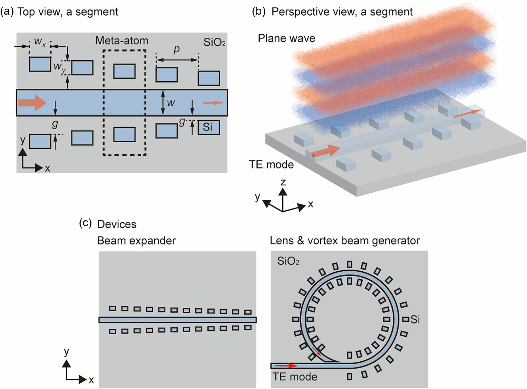
Fig. 1. Schematic diagrams of the amplitude gradient meta-waveguides. (a) A segment of the meta-waveguide consists of a long Si waveguide and cuboid-shaped Si pillars positioned symmetrically by its two sides. All the Si pillars have identical planar dimensions of wx by wy, and they have a constant interval of p along the waveguide. The waveguide-pillar gap g is a critical parameter to control the light scattering amplitude of each meta-atom (highlighted using the dotted line box). (b) By judiciously selecting the values of g, the influence of the power decay in the guided mode (the two red arrows) on light scattering can be compensated, and a plane wave with a large cross section can be created. (c) Two device configurations are considered in this work, where the waveguide is either straight (for plane wave generation) or bent into a circle (for focusing and vortex beam generation).
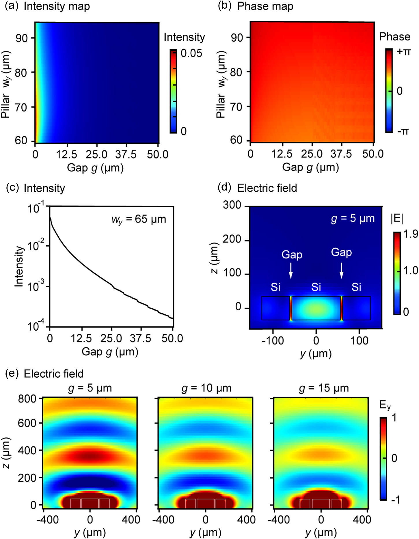
Fig. 2. Light scattering of individual meta-atoms. The value of wx is fixed at 100 μm. (a) Scattering intensity after normalization against the input guided mode, with wy scanned from 60 to 94 μm and g from 0.25 to 50 μm. (b) Scattering phase in the same parameter ranges. (c) Dependence of the output intensity on g with wy fixed at 65 μm. The data are taken from the horizontal line of wy=65 μm in panel (a). (d) Electric field distribution at the yz middle plane of a representative meta-atom, which has wy=65 μm and g=5 μm. The field is normalized against that at the center of the waveguide. (e) The same meta-atom is plotted again at a different scale, and compared against two other meta-atoms. The only geometric difference of these meta-atoms is the value g, which takes three representative values of 5, 10, and 15 μm. All three panels are plotted at the same scale to best visualize the free-space light. As this scale, features of the near field confined to the surface of the meta-atoms are not clearly resolved.
Fig. 3. Off-chip plane wave generation in two amplitude gradient meta-waveguides. In both devices, the input guided mode propagates towards the +x direction, generating a free-space beam that propagates vertically towards the +z direction. The number of meta-atoms is (a) 100 and (b) 1000. Both field maps show an area in the central xz plane, with the bottom edge of the maps one wavelength above the middle plane of the metasurface. The whole length of the two devices is approximately 40 and 400 times the free-space wavelength λ0, and only a section of 25λ0 and 250λ0 is shown here. Due to space constraints, only the first map is plotted to scale. The second map is significantly compressed along the x axis. This compression amplifies any small tilting in the wavefronts in the visualization. (c), (d) Corresponding far field distributions for (c) 100-unit and (d) 1000-unit devices.
Fig. 4. Off-chip light focusing in an amplitude gradient metasurface. (a) Schematic of the device. The waveguide is bent into a circle, and it is decorated uniformly with 100 meta-atoms except for the final 1/12 of the circle. The fundamental TE mode is launched into the waveguide in the +x direction, and each meta-atom functions like an electric dipole radiating in the radial direction. (b) Electric field distribution at the xy plane above the center of the device. The plane passes through the center of the central focal spot, which is approximately 2 mm above the device. (c) Electric field distribution at the xz plane that passes through the center of the device. The bottom edge of the map is 400 μm above the middle plane of the device. (d) Simulated field amplitude along the line of y=0 in panel (b), overlaid with the analytical results derived from a zeroth-order Bessel function of the first kind.
Fig. 5. Off-chip vortex beam emission from four meta-devices. All the devices have the same circular waveguide but a different number of meta-atoms, which is (a) 105, (b) 110, (c) 119, and (d) 128. For each device, the radial electric field Er of the same area is shown here, which is a square of 12 mm×12 mm at approximately 2 mm above the emitter. The field is normalized against the maximal value of the respective figure. The topological charge, which corresponds to the number of optical cycles around the beam axis, is (a) −5, (b) −10, (c) −20, and (d) −30.
Fig. 6. Output of individual meta-atoms, with wx fixed at 65 μm and wy fixed at 100 μm. (a) The intensity decreases nearly exponentially when increasing the gap g; meanwhile (b) the phase is nearly flat in the same range of g.
Fig. 7. Radial electric field of the metalens discussed in Fig. 4 of the main text. The map shows a 2 mm×2 mm square approximately 2 mm above the emitter.
Ref. | Design Approach | Wavelength () | Beam Width (Nominal or Effective) |
---|
[13] | Phase gradient | 1550 nm | (nominal) | [15] | Phase gradient | 720 nm | (effective) | [32] | Phase gradient | 300 μm | (nominal) | This work | Amplitude gradient | 375 μm | (nominal) (effective) |
|
Table 1. Comparison with State-of-the-Art Literature on Meta-Waveguide-Based Plane Wave Generationa