Metasurfaces provide an effective technology platform for manipulating electromagnetic waves, and the existing design methods all highlight the importance of creating a gradient in the output phase across light scattering units. However, in the emerging research subfield of meta-waveguides where a metasurface is driven by guided modes, this phase gradient-oriented approach can only provide a very limited emission aperture, significantly affecting the application potential of such meta-waveguides. In this work, we propose a new design approach that exploits the difference between meta-atoms in their light scattering amplitude. By balancing this amplitude gradient in the meta-atoms against the intensity decay in the energy-feeding waveguide, a large effective aperture can be obtained. Based on this new design approach, three different wavefront shaping functionalities are numerically demonstrated here on multiple devices in the terahertz regime. They include beam expanders that radiate a plane wave, where the beam width can increase by more than 900 times as compared to the guided wave. They also include a metalens that generates a Bessel-beam focus with a width 0.59 times the wavelength, and vortex beam generators that emit light with a tunable topological charge that can reach . This amplitude gradient design approach could benefit a variety of off-chip light shaping applications such as remote sensing and 6G wireless communications.
1. INTRODUCTION
Metasurfaces, also referred to as planar or two-dimensional metamaterials, are ultrathin layers of artificial structures that possess unique electromagnetic functionalities. They enable a high level of control over electromagnetic waves across a broad frequency range that extends from gigahertz to the ultraviolet [1–5]. By imparting a judiciously designed change to the wavefront of these waves, metasurfaces can deflect a light beam towards a designated direction [6,7], and focus it into a diffraction-limited spot [8,9] or along a narrow line [10,11]. It can also convert a simple optical mode (e.g., a linearly polarized plane wave or a fundamental TE mode inside a waveguide) to a far more complicated mode, such as an optical vortex that carries orbital angular momentum (OAM) [12,13] and a hologram that transforms with wavelength [14,15]. In each of these cases, the key to the wavefront shaping has always been considered as identifying a set of meta-atoms (i.e., unit cells of light scatterers) that differ in output phase [16]. For example, in all-dielectric metasurfaces, mechanisms such as the Mie resonance [17–19] and the effective refractive index approximation [19,20] are commonly used in device design, for creating a gradual phase gradient that covers the full cycle. This tuning in the output phase of meta-atoms is often accompanied by a variation in their output amplitude. Although simultaneous control over both the output phase and the output amplitude is feasible for some designs [21–26], most previous works have taken the approach of intentionally suppressing the amplitude variation in meta-atom selection [27]. Because of this dominance of the phase gradient-oriented design approach in metasurface research, “phase gradient metasurface” is viewed widely as a synonym of “gradient metasurface,” sometimes even as a synonym of the term “metasurface” itself.
As opposed to this phase gradient approach, we introduce in this work a different type of metasurfaces that can be referred to as an “amplitude gradient metasurface.” As the name implies, in this type of metasurfaces, the device design emphasizes the amplitude gradient: the meta-atom selection can be purely based on the difference in their light scattering amplitude. As far as we know, this design approach has never been proposed previously.
This amplitude gradient concept is developed for a type of metasurface converter that transforms the guided mode of a waveguide into a free-space mode that propagates off chip [28]. These metasurfaces, which are also referred to as meta-structured waveguides or meta-waveguides [28], possess features of both traditional free-space metasurfaces and leaky-wave antennas, and they represent an emerging subfield of metasurface research. They target applications such as augmented reality displays [29], LiDAR sensing [30], and free-space optical communication [31]. Various wavefront shaping functionalities have been realized on meta-waveguides, including beam deflection [13,32], focusing [13,32–34], as well as the generation of vortex beams [13,34], airy beams [35], and holograms [15,29,36]. Conforming to the statement above, all of these existing metasurfaces [13,15,28–30,32–36] belong to the category of the phase gradient metasurface. This design approach can only offer a limited effective aperture, making power projection over a long distance very difficult. Here, we propose a new, amplitude gradient-oriented design approach, which allows for both a large device aperture and advanced off-chip wavefront shaping.
Sign up for Photonics Research TOC. Get the latest issue of Photonics Research delivered right to you!Sign up now
In the analysis below, the properties of individual meta-atoms and the general principles for their selection are first discussed in Section 2. A number of example devices are then designed and numerically studied, and they show these three distinct wavefront shaping functionalities in the terahertz (THz) regime: beam expansion (in Section 3), focusing (in Section 4), and vortex beam generation (in Section 5). Their main performance characteristics are summarized in Section 6, which also includes a brief discussion on potential experimental challenges and future applications.
2. AMPLITUDE GRADIENT-BASED METASURFACE DESIGN
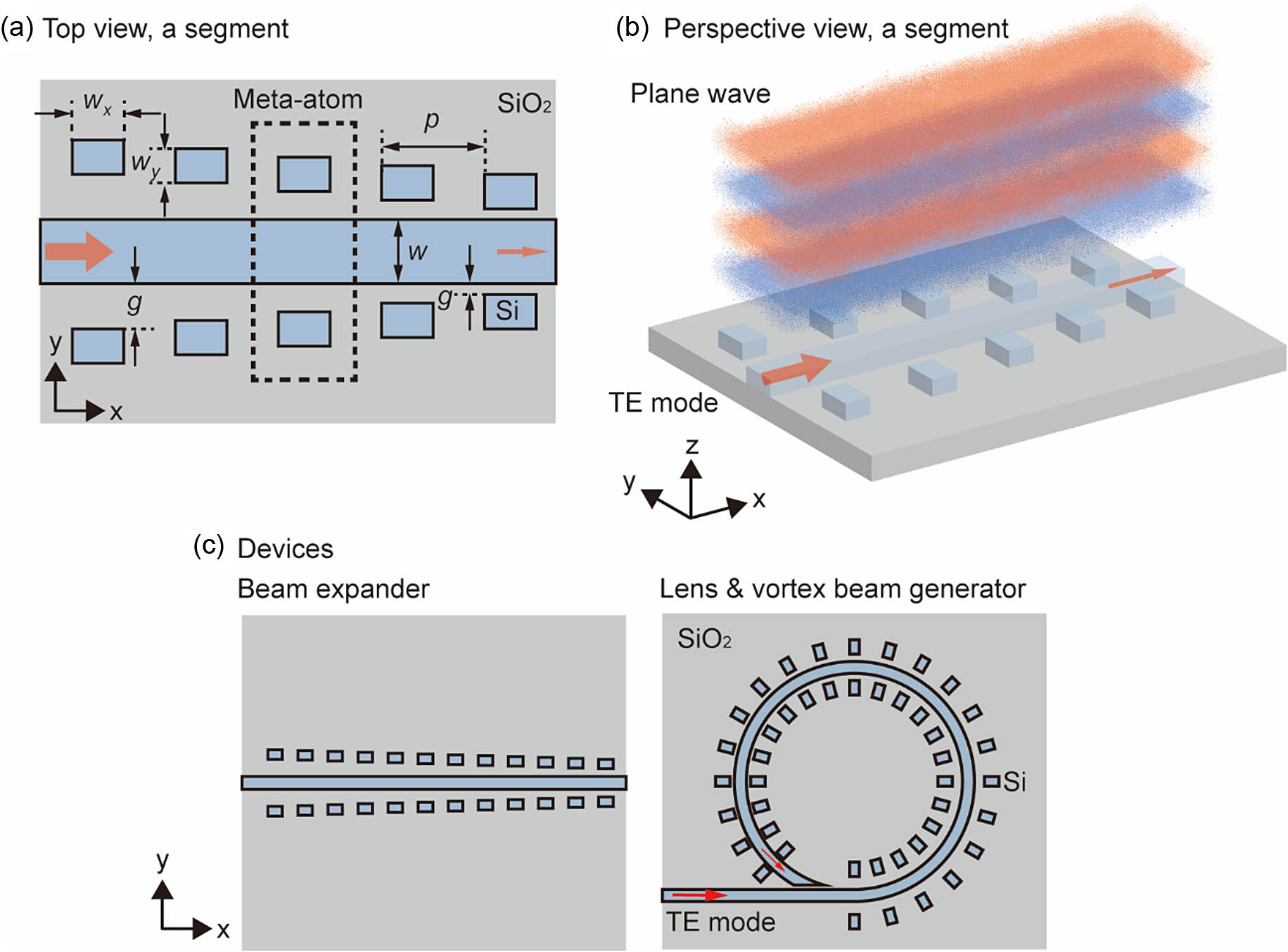
Figure 1 illustrates meta-waveguides designed using the amplitude gradient approach. It shows a top view [Fig. 1(a)] and a perspective view [Fig. 1(b)] of a segment of a meta-waveguide, as well as two kinds of the overall shape of the example devices analyzed in this work [Fig. 1(c)]. The meta-waveguide consists of a long Si waveguide and many pairs of cuboid-shaped Si pillars positioned by its two sides, and the whole structure is on top of a thick layer. The Si waveguide has a rectangular cross section that is in height and in width. All the Si pillars have identical planar dimensions of (along the waveguide direction) and (along the orthogonal direction), and their height is the same as that of the waveguide (i.e., ). The two Si pillars in a pair are placed symmetrically by the two sides of the waveguide, at a constant periodicity of along the waveguide. A meta-atom of this metasurface is consequently a pair of pillars and a segment of waveguide in between [Fig. 1(a)]. The only geometric difference between the meta-atoms is the distance between the waveguide and a side pillar, which is referred to as gap . As will be discussed in detail below, the gap is a critical parameter for the amplitude gradient metasurfaces.
Figure 1.Schematic diagrams of the amplitude gradient meta-waveguides. (a) A segment of the meta-waveguide consists of a long Si waveguide and cuboid-shaped Si pillars positioned symmetrically by its two sides. All the Si pillars have identical planar dimensions of by , and they have a constant interval of along the waveguide. The waveguide-pillar gap is a critical parameter to control the light scattering amplitude of each meta-atom (highlighted using the dotted line box). (b) By judiciously selecting the values of , the influence of the power decay in the guided mode (the two red arrows) on light scattering can be compensated, and a plane wave with a large cross section can be created. (c) Two device configurations are considered in this work, where the waveguide is either straight (for plane wave generation) or bent into a circle (for focusing and vortex beam generation).
A starting point of this amplitude gradient design approach is to position meta-atoms with stronger scattering amplitude (i.e., efficiency) further down the waveguide [Fig. 1(b)]. All meta-waveguides, including both the phase gradient meta-waveguides discussed in previous works [28] and the amplitude gradient meta-waveguides proposed here, are based on scattering a guided mode off chip using a series of meta-atoms. This scattering determines the off-chip wavefront shaping, but also leads to a detrimental shadowing effect [37]. As the residual intensity decreases further down the waveguide, the phase gradient approach always results in a limited effective aperture [28]. By comparison, the amplitude gradient approach proposed here can compensate this shadowing effect and remove this limitation on effective aperture [Fig. 1(b)]. This feature is demonstrated in the first set of example devices in Section 4, where the central waveguide is straight [Fig. 1(c)]. Bending the waveguide into a loop [Fig. 1(c)] can further sculpt the output wavefront into different shapes, which are demonstrated in the second and the third sets of example devices in Sections 5 and 6, respectively.
Figure 2 shows the numerically simulated electromagnetic properties of a set of meta-atoms. The simulation, for this figure and all that followed, was conducted using a commercial finite-difference time-domain solver (FDTD Solutions, Lumerical). Following our recent works on metasurface mode converters [38,39], all of the devices were designed to work at 0.8 THz, which corresponded to a free-space wavelength of 375 μm. Both Si and the underlying were treated as lossless, and their dielectric constants [40,41] were 11.67 and 3.84, respectively. The central Si waveguide was single mode, and had a height of 70 μm and a width of 112 μm. The fundamental transverse electric (TE) mode had an effective index of 2.50, which corresponded to an effective wavelength of 150 μm. For the Si side pillars, their height was set as 70 μm, the same as that of the waveguide. The planar dimensions of , , and were treated as free parameters in device design and analyzed as below.
Figure 2.Light scattering of individual meta-atoms. The value of is fixed at 100 μm. (a) Scattering intensity after normalization against the input guided mode, with scanned from 60 to 94 μm and from 0.25 to 50 μm. (b) Scattering phase in the same parameter ranges. (c) Dependence of the output intensity on with fixed at 65 μm. The data are taken from the horizontal line of μ in panel (a). (d) Electric field distribution at the middle plane of a representative meta-atom, which has μ and μ. The field is normalized against that at the center of the waveguide. (e) The same meta-atom is plotted again at a different scale, and compared against two other meta-atoms. The only geometric difference of these meta-atoms is the value , which takes three representative values of 5, 10, and 15 μm. All three panels are plotted at the same scale to best visualize the free-space light. As this scale, features of the near field confined to the surface of the meta-atoms are not clearly resolved.
Figures 2(a) and 2(b) show the intensity and the phase of light scattered by individual meta-atoms, respectively. In the parametric sweeping, the value of is fixed at 100 μm. The value of is tuned from 60 μm to 94 μm at a step of 1 μm, and is tuned from 0.25 μm to 50 μm at a step of 0.25 μm. The intensity shown in Fig. 2(a) is obtained by integrating the output over a window of 1600 μm (along the waveguide) by 800 μm (in the orthogonal direction), which is located at 480 μm (i.e., slightly over one wavelength) above the center of the meta-atom. The value is very small throughout the whole simulated parameter range [Fig. 2(a)]. Its highest value is only 0.052 after normalization against the input intensity, which occurs at μ and μ (i.e., the smallest value of considered in the simulation). In the whole simulated range of , the intensity rapidly decreases as increases, and appears to be almost zero in Fig. 2(a) once is beyond approximately 10 μm. To show this dependence on more clearly, the values along the horizontal line of μ are extracted from Fig. 2(a) and plotted in Fig. 2(c). The intensity decreases almost exponentially as increases, and varies by over two orders of magnitude in the simulated range of .
In sharp contrast to this exponential dependence of the intensity on gap , the phase shows little sensitivity to both and [Fig. 2(b)]. The values shown in Fig. 2(b) are taken at 480 μm above the center of the meta-atom (i.e., the center of the intensity integration window mentioned above). These phase values are with respect to the input, which is launched at 725 μm before the center of the meta-atom. In the investigation of phase gradient metasurfaces, such phase maps are always plotted over a full range to show the extent of phase coverage [27]. We follow the same style in plotting Fig. 2(b), and obtain here a phase map that appears to be uniform.
To interpret the far-field results of Figs. 2(a)–2(c), Figs. 2(d) and 2(e) show the electric near-field distributions of a few representative meta-atoms. Figure 2(d) shows the electric field at the middle plane of a meta-atom that has μ and μ. Field enhancement is observed in the gaps between the central waveguide and the side pillars, a phenomenon similar to the field confinement observed in Si slot waveguides designed for the telecom wavelength [42]. At the amplitude scale of Fig. 2(d), no scattering field can be discerned due to its small amplitude. To highlight the scattering field, the same field map is plotted at a different scale in Fig. 2(e), where two other meta-atoms are shown together for comparison. The only geometric difference of the three meta-atoms in Fig. 2(e) is in , which is 5, 10, and 15 μm. In all three maps, the scattered wave looks like a spherical wave in the far field and does not reveal the intricate geometry of the meta-atoms. Most importantly, these maps show a clear contrast in the output amplitude and a constant output phase.
The amplitude gradient seen in Fig. 2 is exploited in the following sections, in order to generate a plane wave in Section 3, a focus in Section 4, and a vortex beam that carries a finite value of OAM in Section 5. In Section 3, μ and μ for all meta-atoms. In Sections 4 and 5, the waveguide is bent from a straight line into a circle. To accommodate more pillars along the circle, the values of (now the pillar dimension along the waveguide) and (still the orthogonal planar dimension of the pillars) are swapped in value. In essence, the cuboid Si pillars used in this work are all of the same size, and the different wavefront shaping functionalities are obtained by changing the shape of the waveguide (either a straight line or a circle) and the value of gap .
Before discussing the details of each of the three example functionalities below, it is worth mentioning the influence of the gap dependence shown in Fig. 2(c) on device design. We conducted design optimization in our simulation, and found that for each functionality good results can be obtained by simply adjusting the value of at a constant step, with the smallest positioned at the end of the waveguide. This observation can be understood by considering the absolute scattering power of each meta-atom. For all the devices discussed below, the waveguide can be approximated as a leaky waveguide in which the residual power decreases exponentially with propagation distance. With a constant decrease in along the waveguide, the meta-atoms instead have an almost exponential increase in their scattering efficiency with their distance to the waveguide entrance. These two factors can result in increased uniformity of the output intensity along the waveguide, which underpins the functionalities discussed in the following sections. Regarding the detailed device design, more information is provided in the respective section below, and it is also summarized in Appendix A.
3. BEAM EXPANDER AS THE FIRST FUNCTIONAL DEVICE
In this section, we numerically demonstrate the first functionality obtained by using the amplitude gradient design approach, which is off-chip plane wave generation. The aim here is to expand a guided wave, which is highly constrained in its cross section, into a plane wave with a large beam waist, which can then be further modulated to enable functionalities such as beam steering and focusing. For a waveguide decorated with periodic structures that extends along the axis in the plane (as shown in Fig. 1), we can define a deflection angle for the output light with respect to the vertical direction. This angle can be expressed as [37] where is the free-space wavelength, is the effective wavelength inside the waveguide, is an integer that describes the diffraction order, is the periodicity of the scatterers, and is the phase gradient. Note that this equation is obtained by matching the guided mode and the output light in their in-plane momentum, which brings it to a broad scope of application. It can be applied on different waveguide-driven devices, including phase gradient metasurfaces (where ), conventional gratings (where and all the light scatterers are identical), and the amplitude gradient metasurfaces proposed here (where and all the light scatterers are unique). As here, we can see that if , only one diffraction order of exists, which has a deflection angle . The output light should leave the meta-waveguide vertically into free space. This behavior is confirmed by using the two devices in Fig. 3.
Figure 3.Off-chip plane wave generation in two amplitude gradient meta-waveguides. In both devices, the input guided mode propagates towards the direction, generating a free-space beam that propagates vertically towards the direction. The number of meta-atoms is (a) 100 and (b) 1000. Both field maps show an area in the central plane, with the bottom edge of the maps one wavelength above the middle plane of the metasurface. The whole length of the two devices is approximately 40 and 400 times the free-space wavelength , and only a section of and is shown here. Due to space constraints, only the first map is plotted to scale. The second map is significantly compressed along the axis. This compression amplifies any small tilting in the wavefronts in the visualization. (c), (d) Corresponding far field distributions for (c) 100-unit and (d) 1000-unit devices.
Figure 3 shows the off-chip beam deflection of two meta-waveguides, where the number of meta-atoms is 100 and 1000. Design optimization has been conducted for both devices, with the aim to obtain a flat and horizontal wavefront (details of the meta-atom layout can be found in Appendix A). In the optimization, we have noticed that the meta-atom periodicity needs to be slightly adjusted from the analytical value of 150 μm for a nearly vertical emission. The periodicity is consequently set as 144.5 μm and 149.5 μm for the 100-unit and the 1000-unit devices, respectively. This adjustment in is attributed to the small influence of the side pillars on the effective index of the waveguide, as well as the existence of a small but finite phase gradient [i.e., the in Eq. (1) is not strictly zero].
Figures 3(a) and 3(b) are field maps of the output field along the waveguide direction. Both maps show a plane wave with a nearly flat wavefront and a nearly uniform amplitude. It is worth noting that, due to space constraints, Fig. 3(b) is significantly compressed along the axis. Once the and axes are plotted at the same scale, as in Fig. 3(a), the tilting of the wavefront currently seen in Fig. 3(b) diminishes and becomes barely noticeable.
To quantify the beam deflection performances, the far-field radiation is calculated for both devices and shown in Figs. 3(c) and 3(d). Both radiation maps show a bright spot at the center, congruent to the field maps of Figs. 3(a) and 3(b). Both spots are relatively broad along the axis. This is because only a single waveguide is simulated here for both devices, which already approaches the limit of the computing power available to us. The spots will become narrower along this axis by repeating the same meta-waveguide at a subwavelength interval. Along the axis, detailed analysis reveals that the deflection angle is and 0.08° in Figs. 3(c) and 3(d), respectively, both very close to the target value of 0°. The full width at half maximum (FWHM) of the emission lobe along the axis is 2.41° in Fig. 3(c), and it decreases to 0.26° in Fig. 3(d). This change in the FWHM value originates from an increase in the emission aperture, which accompanies the increase in the number of meta-atoms.
As mentioned in the previous section, as compared to the existing phase gradient design approach, a clear advantage of the amplitude gradient design approach is its capability to compensate energy decay in the energy-feeding waveguide. To highlight this point, we compare our results with the state-of-the-art literature in device aperture in Table 1 [13,15,35]. Here we only consider devices that transform a guided wave to a plane wave, and exclude other forms of off-chip plane wave generation (e.g., generating a plane wave from a surface wave [43]). In the table, we distinguish the nominal width, which is the geometric dimension of a metasurface, from the effective width, which is the size of the beam waist of the emitted light. For our 1000-unit meta-waveguide, the geometric length is , while the beam waist, calculated from the beam FWHM at a height of [i.e., along the top edge of Fig. 3(b)], is . Although the shadowing effect still exists here, our device brings an order of magnitude increase in device aperture as compared to state-of-the-art literature (Table 1). The comparison clearly shows that amplitude gradient metasurfaces are ideal for plane wave generation. As a beam expander, the 1000-unit device increases the beam width by a factor above 900, when we take the waveguide width (i.e., 112 μm) as the width of the input wave. It is worth pointing out that the simulation of the 1000-unit device is close to the limit of our computing power, and we believe that the beam expansion factor can be further increased in the future (e.g., by using larger values of that change at a smaller step).
Comparison with State-of-the-Art Literature on Meta-Waveguide-Based Plane Wave Generationa
Ref.
Design Approach
Wavelength ()
Beam Width (Nominal or Effective)
[13]
Phase gradient
1550 nm
(nominal)
[15]
Phase gradient
720 nm
(effective)
[32]
Phase gradient
300 μm
(nominal)
This work
Amplitude gradient
375 μm
(nominal) (effective)
For the beam width, a nominal value refers to the dimension of the metasurface, while an effective value refers to that of the output light.
4. LIGHT FOCUSING LENS AS THE SECOND FUNCTIONAL DEVICE
Different wavefront shaping functionalities can be obtained simply by bending the straight waveguide shown above into a circle. We explore in this section the focusing function, where the meta-atoms extract the guided light off chip into a focus, and discuss in detail the OAM of the extracted light in the next section. In both sections, as the circle is much larger than individual meta-atoms, the curvature of the central waveguide is ignored in the element selection based on the meta-atom library of Fig. 2.
Figure 4 shows a light focusing circular meta-waveguide, which can also be referred to as a waveguide-driven metalens. The waveguide is bent in the counterclockwise direction [Fig. 4(a)] at an outer radius of 2650 μm. Before tapering off at its tail, the waveguide maintains the same cross-sectional dimensions as those in the previous section (i.e., 70 μm in height and 112 μm in width). The first 11/12 segment of the circle is uniformly decorated with 100 units of meta-atoms. The residual power reaching the end of the metasurface is 10.7% of the total input, while the reflection from the tail that remains inside the waveguide is at the order of .
Figure 4.Off-chip light focusing in an amplitude gradient metasurface. (a) Schematic of the device. The waveguide is bent into a circle, and it is decorated uniformly with 100 meta-atoms except for the final 1/12 of the circle. The fundamental TE mode is launched into the waveguide in the direction, and each meta-atom functions like an electric dipole radiating in the radial direction. (b) Electric field distribution at the plane above the center of the device. The plane passes through the center of the central focal spot, which is approximately 2 mm above the device. (c) Electric field distribution at the plane that passes through the center of the device. The bottom edge of the map is 400 μm above the middle plane of the device. (d) Simulated field amplitude along the line of in panel (b), overlaid with the analytical results derived from a zeroth-order Bessel function of the first kind.
Similar to the devices discussed in the previous section, here the gap is adjusted along the waveguide (see Appendix A for the design details). Its value decreases towards the waveguide tail, creating a gradient in the scattering efficiency in the meta-atoms that compensates the decay in the residual power along the waveguide. The collective response of the meta-atoms creates a circular light source that has an almost uniform intensity distribution along its circumference. This light source approximates an annular aperture, where a ring-shaped opening is cut in an opaque mask. Nevertheless, different from the most standard textbook configuration [44], where an annular aperture is illuminated by a linearly polarized plane wave, here each meta-atom approximates an electric dipole that oscillates in the radial direction [Fig. 4(a)]. This kind of radiation configuration leads to the generation of a Bessel beam, which has been investigated previously in the research field of microring-based vortex beam generators [45].
Figures 4(b) and 4(c) show the output field in a segment of the and planes above this waveguide-driven metalens. An elongated central focus and a series of concentric rings surrounding it are observed, which are key features of a Bessel-beam focus. The field distribution is not perfectly circular in the plane [Fig. 4(b)], which is attributed to factors such as a fluctuation of output intensity along the waveguide, the lack of light scatterers at the end 1/12 segment of the circle, and light scattering at the waveguide tail. The last factor originates from the tapering of the waveguide. A gradual shrink in the waveguide width at its tail reduces light reflection inside the circular waveguide, but it radiates light into free space and can disturb the field distribution at the focus.
To further confirm that the focus is a Bessel beam [46,47], Fig. 4(d) compares the simulated result with a zeroth-order Bessel function of the first kind. A good fitting is observed, especially for the central focal spot. This fitting gives an FWHM of the central focus of 221.2 μm, which is approximately . The output efficiency, taking into account both the central focus and the concentric rings, is 27%.
5. VORTEX BEAM GENERATOR AS THE THIRD FUNCTIONAL DEVICE
The meta-waveguide layout shown in Fig. 4(a), where many light scatterers distribute uniformly along the circumference of a circle, is in fact an ideal configuration for generating optical vortex beams. A vortex beam can carry OAM, which can be utilized for high-resolution imaging [48], laser micromachining [49], particle manipulation [50], as well as optical communication in both the classical and the quantum regimes [51,52]. An analysis on the phase distribution of the output shown in Fig. 4 indeed reveals a finite value of OAM (see Appendix A for details). It is worth noting that, for such radially polarized cylindrical vector vortex beams [53], a focus without an intensity minimum at its center can carry a finite value of OAM [54]. There have been many reports on off-chip vortex beam generation using a waveguide, and they utilize either a phase gradient metasurface or a decorated microring resonator [55–57]. Figure 5 shows that a third approach of off-chip emission exists, which is to use an amplitude gradient metasurface.
Figure 5.Off-chip vortex beam emission from four meta-devices. All the devices have the same circular waveguide but a different number of meta-atoms, which is (a) 105, (b) 110, (c) 119, and (d) 128. For each device, the radial electric field of the same area is shown here, which is a square of at approximately 2 mm above the emitter. The field is normalized against the maximal value of the respective figure. The topological charge, which corresponds to the number of optical cycles around the beam axis, is (a) , (b) , (c) , and (d) .
To understand vortex beam generation using the device layout of Fig. 4(a), we can refer to the vortex beam generation in a decorated microring resonator, where an OAM-carrying vortex beam originates from the phase mismatch between adjacent nanostructures (e.g., shallow holes in Ref. [45]) in their light scattering. The value of the topological charge is consequently derived to be the difference between the number of nanostructures and the resonance order of the whispering gallery mode [45]. Here, we also concentrate on the phase mismatch between adjacent meta-atoms, even though the meta-waveguide does not form a full circle and there is no whispering gallery mode. We consequently can arrive at this expression for the topological charge of : where is the radius of the circle and is the angle between two adjacent meta-atoms. Note that this equation is valid for a meta-waveguide that occupies only a part of a full circle, a configuration that is shared by all four devices in Fig. 5.
Figure 6.Output of individual meta-atoms, with fixed at 65 μm and fixed at 100 μm. (a) The intensity decreases nearly exponentially when increasing the gap ; meanwhile (b) the phase is nearly flat in the same range of .
Figure 5 shows the vortex beams generated by four different devices. The topological charge takes the values of [Fig. 5(a)], [Fig. 5(b)], [Fig. 5(c)], and [Fig. 5(d)], which correspond to the number of optical cycles around the device axis in each map. The waveguide of all these devices is identical to that in the device of Fig. 4. The tuning of the topological charge in Fig. 5 is obtained by adjusting the number of meta-atoms distributed along the circular waveguide, which is 105, 110, 119, and 128 in Figs. 5(a)–5(d), respectively. This adjustment in the number of meta-atoms changes the value of . By taking the same value of 2.523 for all of the devices, the value derived from Eq. (2) is , , , and −30.0 for Figs. 5(a)–5(d), respectively, identical to the simulated results. All four panels of Fig. 5 show the same area at the same height above the devices. It is clear that, as the absolute value of increases from Fig. 5(a) to Fig. 5(d), the radiation becomes more divergent. The output efficiency extracted from Fig. 5 is 29%, 31%, 31%, and 32% for Figs. 5(a)–5(d), respectively.
As two different types of planar vortex beam emitters, the meta-waveguide discussed in this section and the decorated micro-ring resonators [45] have a certain degree of similarity in their device layout. It is thus worth highlighting some of their key differences here. First, the meta-waveguide does not require any whispering gallery mode resonance, which removes a lot of design constraints (e.g., the bus waveguide-ring coupling and the resonance wavelength) and simplifies the design process. Second, the meta-waveguide is more suitable for applications that require a large emission aperture, thanks to its amplitude gradient design approach. (The simulation of the 100-unit devices in Fig. 5 is approaching the limit of our simulation capability, but we foresee that larger devices can also be functional.) Third, unlike the decorated micro-ring resonators, Eq. (2) does not force to be an integer here. Consequently, the meta-waveguide could be utilized as a platform to study the generation of vortex beams that carry a noninteger topological charge [58].
6. CONCLUSION
To conclude, we have proposed and numerically tested a new metasurface design approach for extracting a guided THz wave into free space and shaping its wavefront. The design utilizes meta-atoms with a gradient in their light scattering amplitude, which is achieved by adjusting the size of the gap between the central waveguide and its side pillars. This new amplitude gradient design approach is very different from the widely adopted phase gradient design approach. As this approach can compensate the energy decay in the energy-feeding guided mode, a large number of meta-atoms can be accommodated along a single waveguide, as demonstrated in our 100- and 1000-unit devices. Three different off-chip wavefront shaping functionalities are consequently demonstrated: (1) the generation of a plane wave, where the beam width can reach , equivalently a factor above 900 in width expansion; (2) the generation of a Bessel-beam focus with an FWHM of ; and (3) the generation of OAM-carrying vortex beams, where the topological charge is tuned from to .
The amplitude gradient design concept shown here is generic and can be applied in other regimes, such as microwave and infrared bands, as long as the required tuning in the gap size is within the reach of standard nanofabrication technologies. In future experiments, accurately controlling the gap sizes will be critical, and a potential challenge here is the nanofabrication of devices with a high aspect ratio [59,60]. The device performance can also be affected by factors such as material absorption and surface roughness, which can accelerate the decay of the guided wave and limit the device aperture. Analysis on these factors is beyond the scope of this proof-of-principle demonstration.
The three light shaping functionalities demonstrated here could be used in a range of different applications such as THz imaging [61], molecular sensing [62], and 6G communications [63]. All of the meta-devices demonstrated here have a relatively straightforward configuration of the meta-atoms (all identical and evenly distributed) and the waveguide-pillar gap (changing at a constant step along the waveguide). More complicated configurations (e.g., obtained by incorporating methods such as the inverse design method [64]) could lead to other types of wavefront shaping and functionalities.
Acknowledgment
Acknowledgment. The authors acknowledge the use of the IRIDIS High Performance Computing Facility, and associated support services at the University of Southampton, in the completion of this work.
APPENDIX A: GEOMETRIC PARAMETERS OF ALL THE DEVICES
A total of seven devices (two as beam expanders, one as a metalens, and four as vortex beam generators) have been analyzed in the main text to demonstrate off-chip wavefront shaping. Their geometric parameters, which have been stated in relevant sections in the main text, are summarized here for convenience.
Beam expander: Two devices, one with 100 meta-atoms and the other 1000, are numerically studied. The central waveguide is 70 μm in height and 112 μm in width. The side pillars are 70 μm in height, and the values of (the planar dimension along the waveguide) and (the planar dimension in the orthogonal direction) are 100 μm and 65 μm, respectively. In the 100-unit device, the meta-atoms have a periodicity of 144.5 μm, and the gap decreases from 19.8 μm to 0 at a step of 0.2 μm in the forward direction. In the 1000-unit device, the meta-atom periodicity is 149.5 μm, and the gap decreases from 49.95 μm to 0 at a step of 0.05 μm in the forward direction.
Metalens: A single device that generates a Bessel-beam focus is numerically studied. The central waveguide is bent into a circle at an outer radius of 2650 μm. It remains to be 70 μm in height and 112 μm in width in most part, and it tapers off at its tail. The values of and are swapped to be 65 μm and 100 μm, respectively. One hundred meta-atoms distribute uniformly along the first 11/12 segment of the circle, and the angle between adjacent meta-atoms is 0.05782 rad. The gap decreases at a step of 0.1 μm in the forward direction, and its smallest value is 5 μm.
Vortex beam generator: Four devices with different OAM values are numerically studied. The central waveguide remains unchanged from above (i.e., 2650 μm in outer radius, 70 μm in height, and 112 μm in width). The values of and also remain unchanged (i.e., 65 μm for the former and 100 μm for the latter). In each device, the meta-atoms still distribute uniformly along the first 11/12 segment of the circle. The gap still decreases at a step of 0.1 μm in the forward direction, but its smallest value is now 3 μm. The number of meta-atoms differs among the four devices, which is 105, 110, 119, and 128 in Figs. 5(a)–5(d), respectively. This leads to a variation in the angle , which is 0.05480 rad, 0.05251 rad, 0.04846 rad, and 0.04499 rad in the four panels.
APPENDIX B: META-ATOM OUTPUT WITH wx AT 65?μm AND wy AT 100?μm
Figure 2 of the main text shows the meta-atom output with μ and μ, which is used to design the two beam expanders. By comparison, the dependence on the gap of the output intensity and phase is shown in Fig. 6, with and swapped in value. Similar features are observed here. Consequently, the design of the metalens and the four vortex beam generators follows a procedure similar to that of the beam expanders.
APPENDIX C: OAM OF THE BESSEL-BEAM FOCUS
The Bessel-beam focus shown in Fig. 4 of the main text carries OAM. Its topological charge takes the value of one as revealed in Fig. 7, which is plotted in the same style as that of Fig. 5 of the main text. Note that, as discussed in the main text, the phase singularity of the radial electric field seen here does not contradict with the disc-shaped focus seen in Fig. 4(b).