
Yu Tian, Hailong Wang, Yijia Geng, Lili Cong, Yu Liu, Weiqing Xu, Shuping Xu. Boosting a sub-10 nm nanogap array by plasmon-triggered waveguide resonance[J]. Photonics Research, 2020, 8(12): 1850
- Photonics Research
- Vol. 8, Issue 12, 1850 (2020)
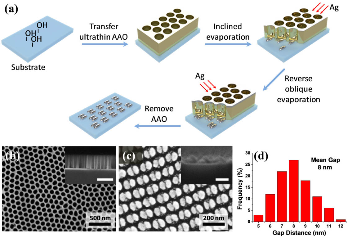
Fig. 1. (a) Preparation process of nanogap arrays; (b) SEM images of the AAO mask. The scale bar of the inset is 500 nm. (c) SEM images of Ag nanogap array. The scale bar of the inset is 100 nm. (d) Statistical results of 100 gap distances.
![(a) Schematic diagram of the polarization direction and nanogap axis; (b) reflectance spectra of the nanogap array in the cases of ⊥ and ∥; (c) and (d) SERS profiles of 4-MBA at different incident angles in the cases of ⊥ and ∥; (e) SERS spectra of 4-MBA on the nanogap array above a silica slide under the resonance angles [65° for case ⊥ and 51° for case ∥, along dashed lines in (c) and (d)].](/richHtml/prj/2020/8/12/12001850/img_002.jpg)
Fig. 2. (a) Schematic diagram of the polarization direction and nanogap axis; (b) reflectance spectra of the nanogap array in the cases of ⊥ ∥ ; (c) and (d) SERS profiles of 4-MBA at different incident angles in the cases of ⊥ ∥ ; (e) SERS spectra of 4-MBA on the nanogap array above a silica slide under the resonance angles [65° for case ⊥ ∥ , along dashed lines in (c) and (d)].
Fig. 3. (a) Schematic diagram and SEM image of the WG; the scale bar is 500 nm. (b) and (c) The measured reflectance spectra of the WG without nanogap array from the prism side and from the air side.
Fig. 4. (a) Schematic diagram of the polarization direction and nanogap axis; (b) measured reflectance spectra of the nanogap array with the WG excited from the air side for the four cases; (c) absorption spectrum of the Ag nanogap array with 8 nm gaps; (d) SERS spectra of a 4-MBA ethanol solution for the four cases; (e) SERS spectra of 4-MBA at different concentrations obtained on Ag nanogap array with the WG in the TE * ∥ cases.
Fig. 5. (a) Schematic diagram of the polarization direction and nanogap axis for the four cases; (b) measured reflectance spectra of the nanogap array with the WG excited from the prism side for the four cases; (c) SERS spectra of a 4-MBA ethanol solution for the four cases; (d) and (e) simulated reflectance spectra and EM field distribution for the four cases, respectively.
Fig. 6. Dark-field images of nanogap array (a) on a silica slide without a WG and (b) on a WG; (c) integral intensity of dark-field images.
Fig. 7. (a) Simulated reflectance spectra for the four cases; (b) simulated EM field distributions for the four cases; (c) comparison of the EM field distributions of the nanogap array with the WG (top row, with 600 nm SiO 2 SiO 2
Fig. 8. Comparisons of the SERS intensities of the nanogap array without the WG and with the WG, including the prism side excitation and the air side excitation.
Fig. 9. (a) EM field distributions of the nanogap array without the WG at different gap distances, ranging from 8 to 3 nm; (b) EM field distribution of 8 nm gap nanogap array with the WG; (c) the strongest EM field at different gap distances, ranging from 8 to 3 nm; (d) integral intensity of the EM field (over 10 times) at different gap distances, ranging from 8 to 3 nm.

Set citation alerts for the article
Please enter your email address
© Copyright 2018-2021 | Chinese Laser Press. All Rights Reserved 沪ICP备15018463号-20