Abstract
High-quality narrow bandgap semiconductors nanowires (NWs) challenge the flexible near-infrared (NIR) photodetectors in next-generation imaging, data communication, environmental monitoring, and bioimaging applications. In this work, complementary metal oxide semiconductor-compatible metal of Ag is deposited on glass as the growth catalyst for the surfactant-assisted chemical vapor deposition of GaSb NWs. The uniform morphology, balance stoichiometry, high-quality crystallinity, and phase purity of as-prepared NWs are checked by scanning electron microscopy, energy dispersive X-ray spectroscopy, high-resolution transmission electron microscopy, and X-ray diffraction. The electrical properties of as-prepared NWs are studied by constructing back-gated field-effect-transistors, displaying a highIon/Ioff ratio of 104 and high peak hole mobility of 400 cm2/(V·s). Benefiting from the excellent electrical and mechanical flexibility properties, the as-fabricated NW flexible NIR photodetector exhibits high sensitivity and excellent photoresponse, with responsivity as high as 618 A/W and detectivity as high as 6.7 × 10¹⁰ Jones. Furthermore, there is no obvious decline in NIR photodetection behavior, even after parallel and perpendicular folding with 1200 cycles.High-quality narrow bandgap semiconductors nanowires (NWs) challenge the flexible near-infrared (NIR) photodetectors in next-generation imaging, data communication, environmental monitoring, and bioimaging applications. In this work, complementary metal oxide semiconductor-compatible metal of Ag is deposited on glass as the growth catalyst for the surfactant-assisted chemical vapor deposition of GaSb NWs. The uniform morphology, balance stoichiometry, high-quality crystallinity, and phase purity of as-prepared NWs are checked by scanning electron microscopy, energy dispersive X-ray spectroscopy, high-resolution transmission electron microscopy, and X-ray diffraction. The electrical properties of as-prepared NWs are studied by constructing back-gated field-effect-transistors, displaying a highIon/Ioff ratio of 104 and high peak hole mobility of 400 cm2/(V·s). Benefiting from the excellent electrical and mechanical flexibility properties, the as-fabricated NW flexible NIR photodetector exhibits high sensitivity and excellent photoresponse, with responsivity as high as 618 A/W and detectivity as high as 6.7 × 10¹⁰ Jones. Furthermore, there is no obvious decline in NIR photodetection behavior, even after parallel and perpendicular folding with 1200 cycles.Introduction
In the past few decades, flexible near-infrared (NIR) photodetectors have attracted significant attention in imaging, data communication, environmental monitoring, and bioimaging applications[1-4]. However, scalability, sensitivity and mechanical stability challenge the selection of channel semiconductors and device fabrication of flexible NIR photodetectors[5]. Due to the excellent mechanical flexibility in comparison to the typical thin film or bulk counterparts, low-dimensional organic and inorganic semiconductors, such as one-dimensional (1D) nanowires (NWs) and two-dimensional nanosheets, have recently been attempted to realize flexible NIR photodetectors[6-11]. Apart from the excellent mechanical flexibility, 1D NWs also have great advantages in large surface-to-volume ratio, high carrier mobility, and good light absorption ability, displaying competitive application in high-sensitive, high-durable and versatile flexible NIR photodetectors[12-17]. For example, flexible CH3NH3PbI3 NW NIR photodetector has been fabricated by Taoet al., displaying a responsivity of 0.227 A/W at the low light intensity of 1 × 10⁸ W/cm2 and maintaining a good photoresponse up to 1500 folding cycles[10]. In the case of inorganic NWs, Bi2O2Se NWs have been adopted to fabricate flexible NIR photodetector by Liet al., demonstrating a remarkable photoresponse and stable characteristics with 1200 bending cycles[8].
Narrow bandgap semiconductors NWs of III−Sb have been considered as promising candidates for next-generation electronic and photoelectronic nanodevices. With the narrow direct bandgap of 0.726 eV and high hole mobility of 1000 cm2/(V·s), GaSb NW is certainly an active channel semiconductor for flexible NIR photodetectors. Up to now, vapor growth methods of molecular beam epitaxy, metal-oxide vapor phase epitaxy, metal-oxide chemical vapor deposition, and chemical vapor deposition (CVD), and so on have been universally developed for the growth of GaSb NWs, followed by the famous vapor–solid–solid or vapor–liquid–solid (VLS) growth mechanism[18-21]. It is worth pointing out that a surfactant-assisted CVD method recently has been developed to prevent the sidewall growth of GaSb NWs, resulting in the successful control of diameter, length, growth orientation, crystallinity, hole concentration and so on[22-26]. During the developed surfactant-assisted CVD process, complementary metal oxide semiconductor (CMOS)-incompatible and -compatible metals of Au, Sn, Pd and Cu have been deposited on substrates to serve as the growth catalysts[22,25-27].
Although the NIR photodetection behavior of GaSb NWs has been studied, there is still very limited work on their flexible photodetectors[25,27,28]. In this work, CMOS-compatible metal of Ag is first adopted as the growth catalyst for GaSb NWs during a surfactant-assisted CVD process. The as-prepared GaSb NWs show high density, smooth surface, balance stoichiometry, uniform diameter and good crystalline. When configuring into the famous back-gated field-effect-transistors (FETs), GaSb NWs exhibit excellent electrical performance with a highIon/Ioff ratio (104) and high peak hole mobility (400 cm2/(V·s)). Additionally, the as-prepared NWs exhibit good NIR photodetection performance, such as high responsivity of 881 A/W, detectivity of 8.5 × 10¹⁰ Jones and fast response speed under 1550 nm illumination. Furthermore, the as-fabricated flexible photodetectors also hold the excellent photoresponse to NIR. After the parallel and perpendicular folding with 1200 cycles, the characteristics of flexible photodetectors exhibit no obvious decline, strongly revealing the promising advantage in robust mechanical flexibility, electrical and photoelectrical stability and bending endurance.
Results and discussion
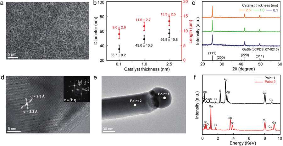
In this work, CMOS-compatible metal of Ag is deposited on amorphous glass as the growth catalyst during the developed surfactant-assisted CVD process. The detailed growth process can be found in supplementary material. From the scanning electron microscopy (SEM) image inFig. 1(a) and Fig. S1, all the as-prepared samples are uniform NWs with high density and smooth surfaces. As shown inFig. 1(b), as the thickness of Ag catalyst films increases from 0.1, 1.0, to 2.5 nm, the diameter of as-prepared NWs increases from 35.7 ± 9.2, 49.0 ± 10.6, to 56.8 ± 10.8 nm, while the corresponding length increases from 9.0 ± 2.6, 11.6 ± 2.7 to 13.3 ± 2.5μm. All of the diameters and lengths are estimated from the corresponding SEM images, as shown in Fig. S1. As verified by X-ray diffraction (XRD) inFig. 1(c), the as-prepared NWs are the pure zinc blende crystal structure (JCPDS Card No. 07–0215) of GaSb. Furthermore, high-resolution transmission electron microscope (HRTEM) is adopted to characterize the microstructure of Ag-catalyzed GaSb NWs. The clear lattice spacings of 2.2 Å are assigned to (
) and (
) planes, indicating the good crystallinity of as-prepared GaSb NW grows along
direction. This result is further confirmed by the corresponding reciprocal lattice space extracted by fast Fourier transform (FFT). At the same time, a spherical catalytic seed is observed on the tip of NW (as shown inFig. 1(e)), inferring a VLS growth mechanism[22,26]. The composition of catalytic seed and NW body are then checked by energy dispersive X-ray spectroscopy (EDS) inFig. 1(f). The spherical catalytic seed contains Ag, Ga and S elements, whereas the NW body shows a balanced stoichiometry of Ga : Sb ~ 1 : 1. In other words, high-quality GaSb NWs with controlled diameters and lengths are prepared successfully by using CMOS-compatible metal of Ag as the growth catalyst during a surfactant-assisted CVD process.

Figure 1.(Color online) Controllable growth of GaSb NWs by using the CMOS-compatible metal of Ag as the growth catalyst. (a–c) SEM image, diameter and length statistics, and XRD patterns of as-prepared Ag-catalyzed GaSb NWs. (d) HRTEM image of GaSb NW, insert is FFT image. (e) Scanning TEM image of an individual GaSb NW. (f) EDS of NW tip and body.
Table Infomation Is Not Enable
After the successful growth of high-quality GaSb NWs, back-gated FETs are constructed to investigate the corresponding electrical properties, as shown inFig. 2. The linear output characteristic ofFig. 2(a) confirms the ohmic-like contact of as-constructed GaSb NWFET with Ni electrodes. As depicted inFig. 2(b) and Fig. S2, the typical transfer curve exhibits the p-type conduction behavior of as-prepared Ag-catalyzed GaSb NW with a highIon/Ioff ratio of 104, which is similar to the previous reports[21,25]. The hysteresis observed in the transfer curve may be caused by the surface states or dielectric interfaces, which could be weakened further by surface decoration or passivation, construction of core-shell structure and introduction of stress, and so on[29-33]. The field-effect mobility of as-constructed back-gated NWFET is then calculated by the square law model. The field-effect mobilityμ can be calculated fromμ =gm × (L2/COX) × (1/VDS), wheregm is the low-bias (i.e.,VDS = 0.1 V) transconductance extracted from the transfer characteristicsgm = (dIDS)/(dVGS )|VDS, in whichL is the channel length, andCOX is the gate capacitance obtained from the finite element analysis software COMSOL for different NW diameters[25,29,34,35]. In this case, as shown inFig. 2(c), the corresponding peak hole mobility reaches up to 400 cm2/(V·s), with NW diameter of 30 nm and channel length of 5μm, approaching to the theoretical mobility limitation with a hole concentration of 1018 cm–3[36]. In addition, it is worth pointing out that a wire-to-wire variation is observed in peak hole mobility statistic ofFig. 2(d), contributing from the dependence of electrical properties on NW diameters, orientations, surface roughness and others. Nevertheless, the as-prepared Ag-catalyzed GaSb NWs exhibit impressive electrical performance, promising the next-generation electronic devices.
Figure 2.(Color online) Electrical properties of the as-prepared Ag-catalyzed GaSb NWs. (a, b) Output and transfer characteristics of as-constructed GaSb NWFET. The inset is the corresponding device schematics. (c) Hole mobility of the corresponding NWFET. (d) Peak hole mobility statistic of as-constructed NWFETs.
Benefiting from the narrow bandgap, the NIR photodetection behaviors of as-prepared Ag-catalyzed GaSb NWs are then systematically investigated by constructing the famous metal-semiconductor-metal devices on a hard substrate. TheI–t curves of GaSb NW photodetectors under different illuminations of λ = 850 nm to λ = 1550 nm are presented inFig. 3(a) and Figs. S3(a)–S3(c). Although fluctuation is observed, it is clear that the photocurrent (defined asIph = |Ilight| − |Idark|) is effectively modulated by periodic monochromatic laser illumination, which reveals that the as-fabricated photodetector shows excellent photoresponse to NIR bands and reproducible dynamic stability.Fig. 3(b) depicts the dependent relationship of the photocurrent on the incident light power intensity which obeys the power lawIph ~Pβ, whereIph is the photocurrent,P is the light intensity andβ is the empirical value[37-39]. Therefore,β = 0.23, 0.24, and 0.24 are fitted by the relationships according to the data of 850, 1310, and 1550 nm, respectively. Because the wavelength of incident lights is much larger than the diameter of NWs, the absorption difference of NWs under the illuminations of three incident lights is neglectable, resulting in the similar values ofβ. It is worth pointing out that the value ofβ reflects the complex process of electron-hole generation, trapping, and recombination within the NW[39,40]. Meanwhile, the GaSb NW photodetectors also display good static detection performance, as shown in Fig. S3(d). Therefore, further efforts can be focused on the current fluctuation suppressing by surface passivation or the construction of core-shell NWs[30,41,42].
Figure 3.(Color online) NIR photodetection behaviors of as-prepared Ag-catalyzed GaSb NWs. (a)I–t curves of GaSb photodetector under different illuminations of λ = 850 nm to λ = 1550 nm at 0.1 V. (b, c) Incident light intensity-dependent photocurrent, responsivity and detectivity, respectively. (d) Rise and decay time of the as-fabricated photodetector under 1550 nm laser illumination.
Notably, responsivity (R) and detectivity (D*) are two essential parameters for a photodetector,R indicates the response efficiency of the photodetector to the optical signal andD* characterizes the minimum light signal that the photodetector can detect[31,42].R can be defined asR =Iph/(PA), in whichIph is the photocurrent,P is the incident power density, andA is the effective irradiated area of the corresponding photodetector.D* can be defined asD* =RA1/2/(2eIdark)1/2, wheree is the electronic charge andIdark is dark current[38]. In this case, as shown inFig. 3(c), theR reaches up to 881 A/W and theD* reaches up to 8.5 × 10¹⁰ Jones under the illumination of 1550 nm laser with an intensity of 0.57 mW/mm2, whileR andD* reach 1059 A/W, 1.1 × 10¹¹ Jones and 1661 A/W, 1.8 × 10¹¹ Jones for the NIRs of 1310 and 850 nm, respectively. Furthermore, another essential parameter for photodetector is the response time, which can be defined as the rising time (τr) and decay time (τd) for the photocurrent to increase/decrease from 10/90% to 90/10%, respectively[25,42]. From the temporal photoresponse curve of GaSb NW photodetector under the illumination of 1550 nm laser inFig. 3(d), theτr can be calculated as 11 ms and theτd can be calculated as 16 ms. In short, the as-fabricated Ag-catalyzed GaSb NW NIR photodetector exhibits excellent photoresponse performance on a hard substrate, promising the next-generation photoelectric devices.
With the excellent photodetection performance, it is necessary to make use of as-prepared Ag-catalyzed GaSb NWs to fabricate flexible NIR photodetectors. In general, the surface roughness of flexible substrates is challenging the fabrication of high-performance NIR photodetectors[2,6]. After the optimization of photolithography process, GaSb NW flexible photodetectors on polyimide (PI) substrates are successfully fabricated, as shown inFig. 4(a). The as-fabricated GaSb NW flexible photodetectors exhibit good bendability and flexibility, and even maintain good shape at bending radius of 3 mm as shown inFig. 4(a). As presented inFig. 4(b), the GaSb NW flexible photodetector shows good and stable photoresponse to NIR lasers of different wavelengths before bending. The R is as high as 618 A/W andD* is as high as 6.7 × 10¹⁰ Jones under the illumination of 1550 nm laser, as shown in Fig. S4(a), which is comparable to the performance of device on hard substrate. It is worthwhile to note that even under the small bias of 0.1 V, the as-fabricated GaSb NW photodetector still exhibits competitive NIR photodetection performances on both hard and flexible substrates, as shown inTable 1. The photodetection performance of flexible GaSb NWs photodetectors can be further optimized by using the smoother and softer flexible substrates[6,28]. Apart from flexibility, the bending endurance is another indispensable factor restricting the development and practical application of the flexible devices[12,45,46]. To more realistically test the bending endurance, the flexible photodetector is bent in parallel and perpendicular orientation alternatively, as shown inFig. 4(c). It is obviously that the photodetection performance of GaSb NW flexible photodetector shows no obvious decline after the multiple bending cycles. Even after bending with 1200 cycles, the GaSb NW flexible photodetector still maintains satisfactory detection performance for 850, 1310, and 1550 nm NIR lights as shown in Figs. S4(b) and S4(c). These results reveal that the as-fabricated flexible NIR photodetector enabled by Ag-catalyzed GaSb NW exhibits outstanding mechanical flexibility, photoelectronic stability and bending endurance, greatly promoting the development of NWs flexible photodetectors.
Figure 4.(Color online) NIR photodetection behaviors of as-fabricated GaSb NW flexible photodetector. (a) The photographs of as-fabricated flexible photodetector under different bending radius. (b) The time-resolved photoresponse of flexible photodetector under the illuminations of 850, 1310, and 1550 nm lasers with 0.1 V bias before bending. (c) The time-resolved photoresponse of photodetector under the illumination of 1550 nm laser after bending different cycles.
Conclusion
In summary, high-quality GaSb NWs have been prepared successfully by adopting the CMOS-compatible metal of Ag as the growth catalyst during a surfactant-assisted CVD process. The as-prepared NWs show high density, smooth surface, balance stoichiometry, uniform diameter and good crystallinity. They also exhibit the expected high peak hole mobility of 400 cm2/(V·s), high responsivity of 881 A/W, high detectivity of 8.5×10¹⁰ Jones and fast response speed under the illumination of 1550 nm. When configured into the flexible photodetectors, GaSb NWs have excellent NIR photodetection behaviors, along with high mechanical flexibility and bending endurance. All of these results promote the use of as-studied high-quality GaSb NWs catalyzed by Ag for the next-generation high-performance flexible NIR photodetectors.
Appendix A. Supplementary material
Supplementary materials to this article can be found online athttps://doi.org/10.1088/1674-4926/43/11/112302.
References
[1] W H Ran, L L Wang, S F Zhao et al. An integrated flexible all-nanowire infrared sensing system with record photosensitivity. Adv Mater, 32, 1908419(2022).
[2] S L Wei, F Wang, X M Zou et al. Flexible quasi-2D perovskite/IGZO phototransistors for ultrasensitive and broadband photodetection. Adv Mater, 32, 1907527(2020).
[3] Z Y Li, S Trendafilov, F L Zhang et al. Broadband GaAsSb nanowire array photodetectors for filter-free multispectral imaging. Nano Lett, 21, 7388(2021).
[4] S Yip, L F Shen, J C Ho. Recent advances in flexible photodetectors based on 1D nanostructures. J Semicond, 40, 111602(2019).
[5] C Xie, F Yan. Flexible photodetectors based on novel functional materials. Small 2017, 13, 822(1701).
[6] Z Lou, G Z Shen. Flexible photodetectors based on 1D inorganic nanostructures. Adv Sci, 3, 1500287(2016).
[7] P Li, Q Y Hao, J D Liu et al. Flexible photodetectors based on all-solution-processed Cu electrodes and InSe nanoflakes with high stabilities. Adv Funct Mater, 32, 2108261(2021).
[8] J Li, Z X Wang, J W Chu et al. Oriented layered Bi2O2Se nanowire arrays for ultrasensitive photodetectors. Appl Phys Lett, 114, 151104(2019).
[9] D J Wu, H Zhou, Z H Song et al. Welding perovskite nanowires for stable, sensitive, flexible photodetectors. ACS Nano, 14, 2777(2020).
[10] J Y Tao, Z J Xiao, J F Wang et al. A self-powered, flexible photodetector based on perovskite nanowires with Ni-Al electrodes. J Alloys Compd, 845, 155311(2020).
[11] Z Lou, X L Yang, H R Chen et al. Flexible ultraviolet photodetectors based on ZnO–SnO2 heterojunction nanowire arrays. J Semicond, 39, 024002(2018).
[12] D P Li, S Yip, F Z Li et al. Flexible near-infrared InGaSb nanowire array detectors with ultrafast photoconductive response below 20 µs. Adv Opt Mater, 8, 2001201(2020).
[13] M Rezaei, S Bianconi, L Lauhon et al. A new approach to designing high-sensitivity low-dimensional photodetectors. Nano Lett, 21, 9838(2021).
[14] E Barrigon, M Heurlin, Z Bi et al. Synthesis and applications of III-V nanowires. Chem Rev, 119, 9170(2019).
[15] X M Yuan, D Pan, Y J Zhou et al. Selective area epitaxy of III–V nanostructure arrays and networks: growth, applications, and future directions. Appl Phys Rev, 8, 021302(2021).
[16] X R Zuo, Z Y Li, W W Wong et al. Design of InAs nanosheet arrays with ultrawide polarization-independent high absorption for infrared photodetection. Appl Phys Lett, 120, 071109(2022).
[17] Z Q Zhong, X L Li, J Wu et al. Wavelength-tunable InAsP quantum dots in InP nanowires. Appl Phys Lett, 115, 053101(2019).
[18] X H Ji, X G Yang, T Yang. Self-catalyzed growth of vertical GaSb nanowires on InAs stems by metal-organic chemical vapor deposition. Nanoscale Res Lett, 12, 428(2017).
[19] L J Wen, D Pan, D X Liao et al. Foreign-catalyst-free GaSb nanowires directly grown on cleaved Si substrates by molecular-beam epitaxy. Nanotechnology, 31, 155601(2020).
[20] M Jeppsson, K A Dick, H A Nilsson et al. Characterization of GaSb nanowires grown by MOVPE. J Cryst Growth, 310, 5119(2008).
[21] Y X Yin, Y N Guo, D Liu et al. Substrate-free chemical vapor deposition of large-scale Ⅲ-Ⅴ nanowires for high-performance transistors and broad-spectrum photodetectors. Adv Opt Mater, 10, 2102291(2022).
[22] Z X Yang, N Han, M Fang et al. Surfactant-assisted chemical vapour deposition of high-performance small-diameter GaSb nanowires. Nat Commun, 5, 5249(2014).
[23] Z X Yang, Y X Yin, J M Sun et al. Chalcogen passivation: an in-situ method to manipulate the morphology and electrical property of GaAs nanowires. Sci Rep, 8, 6928(2018).
[24] Z X Yang, L Z Liu, S Yip et al. Complementary metal oxide semiconductor-compatible, high-mobility, 111-oriented GaSb nanowires enabled by vapor-solid-solid chemical vapor deposition. ACS Nano, 11, 4237(2017).
[25] J M Sun, M Peng, Y S Zhang et al. Ultrahigh hole mobility of Sn-catalyzed GaSb nanowires for high speed infrared photodetectors. Nano Lett, 19, 5920(2019).
[26] N Han, Y Wang, Z X Yang et al. Controllable Ⅲ-Ⅴ nanowire growth via catalyst epitaxy. J Mater Chem C, 5, 4393(2017).
[27] T Luo, B Liang, Z Liu et al. Single-GaSb-nanowire-based room temperature photodetectors with broad spectral response. Sci Bull, 60, 101(2015).
[28] K Zhang, R Q Chai, R L Shi et al. Self-catalyzed growth of GaSb nanowires for high performance ultraviolet-visible-near infrared photodetectors. Sci China Mater, 63, 383(2019).
[29] J M Sun, X M Zhuang, Y B Fan et al. Toward unusual-high hole mobility of p-channel field-effect-transistors. Small, 17, 2102323(2021).
[30] D Liu, F J Liu, Y Liu et al. Schottky-contacted high-performance GaSb nanowires photodetectors enabled by lead-free all-inorganic perovskites decoration. Small, 18, 2200415(2022).
[31] J S Miao, W D Hu, N Guo et al. Single InAs nanowire room-temperature near-infrared photodetectors. ACS Nano, 8, 3628(2014).
[32] S Al-Zahrani, J Pal, M A Migliorato et al. Piezoelectric field enhancement in III-V core–shell nanowires. Nano Energy, 14, 382(2015).
[33] J Holmer, L Zeng, T Kanne et al. Enhancing the nir photocurrent in single GaAs nanowires with radial p-i-n junctions by uniaxial strain. Nano Lett, 21, 9038(2021).
[34] A C Ford, J C Ho, Y L Chueh et al. Diameter-dependent electron mobility of InAs nanowires. Nano Lett, 9, 360(2009).
[35] R A Burke, X J Weng, M W Kuo et al. Growth and characterization of unintentionally doped GaSb nanowires. J Electron Mater, 39, 355(2010).
[36] D Kranzer. Mobility of holes of zinc-blende III-V and II-VI compounds. Phys Status Solidi A, 26, 11(1974).
[37] J S Jie, W J Zhang, Y Jiang, al at. Photoconductive characteristics of single-crystal CdS nanoribbons. Nano Lett, 6, 1887(2006).
[38] H H Fang, W D Hu, P Wang et al. Visible light-assisted high-performance mid-infrared photodetectors based on single InAs nanowire. Nano Lett, 16, 6416(2016).
[39] H Kind, H Q Yan, B Messer et al. Nanowire ultraviolet photodetectors and optical switches. Adv Mater, 14, 158(2002).
[40] X Liu, L L Gu, Q P Zhang et al. All-printable band-edge modulated ZnO nanowire photodetectors with ultra-high detectivity. Nat Commun, 5, 4007(2014).
[41] D S Zheng, J L Wang, W D Hu et al. When nanowires meet ultrahigh ferroelectric field-high-performance full-depleted nanowire photodetectors. Nano Lett, 16, 2548(2016).
[42] L Liu, L M Wu, A W Wang et al. Ferroelectric-gated InSe photodetectors with high on/off ratios and photoresponsivity. Nano Lett, 20, 6666(2020).
[43] Z H Ren, P Wang, K Zhang et al. Short-wave near-infrared polarization sensitive photodetector based on GaSb nanowire. IEEE Electron Device Lett, 42, 549(2021).
[44] K Zhang, Z H Ren, H C Cao et al. Near-infrared polarimetric image sensors based on ordered sulfur-passivation GaSb nanowire arrays. ACS Nano, 16, 8128(2022).
[45] Z Liu, G Chen, B Liang et al. Fabrication of high-quality ZnTe nanowires toward high-performance rigid/flexible visible-light photodetectors. Opt Express, 21, 7799(2013).
[46] Y Yao, W Huang, J H Chen et al. Flexible complementary circuits operating at sub-0.5V via hybrid organic-inorganic electrolyte-gated transistors. Proc Natl Acad Sci USA, 118, 44(2021).