Abstract
Color centers in diamond—especially group IV defects—have been advanced as a viable solid-state platform for quantum photonics and information technologies. We investigate the photodynamics and characteristics of germanium-vacancy (GeV) centers hosted in high-pressure high-temperature diamond nanocrystals. Through back-focal plane imaging, we analyze the far-field radiation pattern of the investigated emitters and derive a crossed-dipole emission, which is strongly aligned along one axis. We use this information in combination with lifetime measurements to extract the decay rate statistics of the GeV emitters and determine their quantum efficiency, which we estimated to be ~ ( 22 ± 2 ) % . Our results offer further insight into the photodynamic properties of the GeV center in nanodiamonds and confirm its suitability as a desirable system for quantum technologies.1 Introduction
Single emitters in diamond, especially group IV color centers, have been identified as suitable hardware for many solid-state-based quantum applications—including quantum networks, quantum information processing, and sensing.1–10 This is largely due to their favorable optical properties, such as narrow zero-phonon line (ZPL) emission and low spectral diffusion.11–15 These characteristics arise from the split-vacancy configuration of group IV diamond centers with the foreign atom (Si, Ge, Sn, and Pb) occupying an interstitial site between two carbon vacancies along the direction in the diamond lattice.16–22 The corresponding inversion symmetry of the defects grants them a vanishing permanent electric dipole moment and thus renders the optical transition frequency insensitive to first-order electric-field and strain variations.
Recent studies have focused predominantly on the germanium-vacancy (GeV) defect, which has been successfully engineered using both chemical vapor deposition, high-pressure high-temperature (HPHT), and ion implantation techniques.17,23–26 The defect has a zero phonon line around 602 nm, which splits into four lines at cryogenic temperatures.6 The successful incorporation of GeV defects into photonic resonators and plasmonic waveguides has also been demonstrated.27,28 However, despite the rapid progress, the photophysical properties of the GeV centers in nanodiamonds (NDs) are still poorly understood.
In this work, we characterize the photodynamics of GeV centers hosted in HPHT NDs, both in ensemble and single-emitter measurements. We perform photoluminescence (PL) and lifetime spectroscopy analyses and use Fourier-plane imaging to determine the far-field radiation pattern of the emitters. We then combine these results to produce an approximated estimate of the quantum efficiency (QE) of an ensemble of GeV emitters. We achieve this by mapping the emitters’ radiative component () of their total decay rate () onto changes in the emitters’ PL lifetime as we control their dielectric surrounding environment.29,30
Sign up for Advanced Photonics TOC. Get the latest issue of Advanced Photonics delivered right to you!Sign up now
2 Materials and Methods
The NDs containing GeV centers were fabricated via HPHT at the Institute for High Pressure Physics, Russian Academy of Sciences, Moscow.31 The process involved the use of naphthalene () mixed with germanium, under 8 to 9 GPa of pressure and at temperatures , and resulted in high-quality ND crystals (size ), containing Ge-related color centers, including germanium-vacancy (GeV) centers.
For characterization, we dispersed the NDs on a transparent glass coverslip (, thickness 0.13 to 0.16 mm; Ted Pella), which had been laser scribed with a unit grid consisting of squares to facilitate the identification and localization of target emitters. We performed the optical characterization using a lab-built confocal microscope, with confocality achieved via a lens system and a pinhole (diameter ) positioned within the collection path. Excitation of the emitters and collection of their PL signal was carried out using a 1.4 numerical aperture oil immersion objective. Spectroscopy, lifetime, and second-order autocorrelation measurements were carried out using a spectrometer (Acton SpectraPro, equipped with a PIXIS 256 camera; Princeton Instruments) and two avalanche photodiodes (Count T; Laser Components) arranged in a Hanbury–Brown and Twiss interferometer connected to a correlator (TimeTagger 20; Swabian). We used a 532-nm continuous-wave (cw) laser (SPL-532, Shanghai Dream Lasers Technology) as the primary excitation source for all optical experiments, and we employed a 512-nm pulsed laser (PiL051-FS, Advanced Laser Diode Systems GmbH) for the lifetime measurements. We probed the samples in cw at an intensity measured at the back aperture of the objective of while pulsed excitation was performed under an average power of , with a repetition rate of 20 MHz. Fourier plane imaging was performed through an additional optical pathway utilizing a lens configuration and magnification at the EMCCD camera (Oxford Instruments iXon Ultra 888). We determined the size of the individual diamond nanoparticles via atomic force microscopy (AFM, XE7; Park Systems).
To fit the back focal plane (BFP) images, we first analytically calculated the sum of two BFP intensity distributions originating from crossed linear dipoles positioned above a glass cover slide using the equations from Ref. 32. The residues to the experimental data were minimized using the sequential least squares programming algorithm with four free parameters: the in-plane angle () and the out-of-plane angle () of one dipole, the rotation angle of the perpendicularly oriented dipole, and the relative amplitude of the two dipoles.
3 Results and Discussions
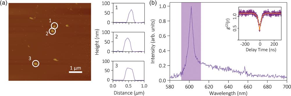
We characterized NDs containing either ensembles or single GeV centers. Figure 1(a) is the AFM image of the investigated NDs, which are , and Fig. 1(b) shows their PL spectrum. The sharp peak at corresponds to the ZPL emission wavelength of the GeV center. The inset in Fig. 1(b) displays the second-order autocorrelation measurement, , which was used to identify single emitters, . For this particular emitter, the value was measured to be (), evaluated with a timing jitter of 500 ps.

Figure 1.NDs containing GeV color centers. (a) AFM image showing the typical size of the NDs. The numbered white circles refer to the corresponding height profiles. (b) Characteristic PL spectrum of a typical ND containing GeV color center(s) with ZPL at 602 nm. Inset: second-order autocorrelation function indicating emission from a single GeV, . The purple shading in the spectrum indicates the band of wavelengths selected by the bandpass filter in the autocorrelation measurement.
We then performed a detailed analysis of the radiation pattern of GeV emitters as shown in Fig. 2. Specifically, we used a optical relay system to image the BFP of the objective onto an EMCCD camera (cf. Sec. 2). The corresponding light intensity distribution is representative of the far-field radiation pattern of the emitter and can thus be used to map the in-plane angle () and the out-of-plane angle () of the emitting dipole(s) in the sample plane. For each GeV color center, we expect a crossed-dipole far-field radiation pattern where the dipole moment aligned along the symmetry axis of the defect is dominating.33 This, however, has never been shown experimentally thus far. Figure 2 shows the experimental [Fig. 2(a)] and calculated [Fig. 2(b)] BFP radiation pattern for three typical NDs containing each a single GeV center. The theoretical fit to the experimental BFP images highlights that the intensity distributions are consistent with the expected crossed-dipole emission, dominated by a single dipole moment. The calculated, best-fit-to-the-data values for the angles and of the crossed dipoles (cf. Sec. 2) are indicated. Since the characterized GeV defects embedded in NDs are randomly distributed with respect to the glass surface, it is expected that both and will vary from crystal to crystal. Note that before each measurement, the single photon nature of the GeV center was confirmed using second-order autocorrelation measurements.
Figure 2.BFP analysis of three individual GeV single-photon emitters. (a) BFP images measured experimentally for each individual emitter. (b) Corresponding simulated 2-D dipole fits. The fitted in-plane () and out-of-plane () angles of the crossed dipole (subscripts 1 and 2) for each GeV center are indicated explicitly.
We also performed an analysis on the emission properties of fluorescent NDs hosting single GeV emitters. Figure 3 illustrates our findings. The photoemission from individual centers is stable [Fig. 3(a)] and reaches saturation intensities of to [Fig. 3(b)]. The single emitter in Fig. 3(b) is representative of the surveyed emitters. It displays a saturation intensity —determined as with being the excitation power at saturation. Figure 3(c) summarizes the distribution of lifetimes measured for 18 individual NDs containing GeV centers; Figs. 3(d) and 3(e) show the distribution of their ZPL emission wavelength and full width at half maximum (FWHM). The measured lifetimes varied substantially among centers spanning over the range to 25 ns [Fig. 3(c)], with an average value of and consistent with previous reports.28 The lifetime of the GeV defect in bulk diamond has been measured to be to 5.5 ns.17,26 Considerably long lifetimes in NDs are expected for some color centers, e.g., the nitrogen vacancy (NV) center.34 The NV possesses a noninversion symmetry and thus fluctuating electromagnetic fields (e.g., due to traps on the diamond surface) may influence its lifetime significantly. On the other hand, the SiV defect in NDs exhibits very similar values of measured lifetime ( to 2 ns), even in NDs just a few nm in size.35 The fact that the GeV center shows more variability in lifetime values than the SiV—despite sharing the same crystallographic symmetry—has been suggested to derive from its higher QE. A higher QE would make the GeV more sensitive to changes in the local photonic density of states, resulting in the lifetime varying more widely from ND to ND.
Figure 3.Summary of the optical properties of characteristic NDs containing GeV centers. (a) Kinetic spectra measurement of a single GeV emitter, showing photostable emission at 604 nm (FWHM ~ 4.27 nm) for 500 s at 10-s integration time intervals. (b) Saturation measurement of the emitter. The extracted saturation intensity is . (c) Histogram of the emitter lifetime. (d) Histogram of emitter ZPL position. (e) Histogram of FWHMs of the fitted ZPLs. The dotted lines represent the average values of their respective dataset. Each histogram represents a sample size of 18 individual emitters.
Finally, we discuss a method to determine the QE of GeV centers hosted in diamond nanoparticles. On average, the GeV center is brighter than the SiV, as was reported by numerous groups.6,26,36 However, the value of the QE was never determined experimentally. The method to determine the QE relies on modifying, in a controlled manner, the electromagnetic interaction between the emitters and the surrounding dielectric environment. In general, the total decay rate () of an emitter is given by the sum of its radiative () and nonradiative () components, with the ratio determining the emitter’s QE. Of these decay rates, only the radiative one () depends on the local density of states (LDOS). We can therefore design an experiment in which we alter deterministically the LDOS and indirectly extract the value of from the corresponding change in the excited state lifetime, .30 Specifically, for an emitter in an unbounded dielectric medium of refractive index , the transition probability is governed by Fermi’s golden rule , where is the decay rate in vacuum—so long as the emitter is at a distance from any dielectric interface. For , the spontaneous emission rate can be determined from (and strongly depends on) the distance , the dipole orientation (polar angle with respect to the normal to the interface), and the refractive indexes at the interface. Conversely, the nonradiative decay rate is assumed constant, regardless of . This means that the PL lifetimes measured for the same emitter located close to () or far from () a dielectric interface should vary due solely to a difference in the rate . This ultimately allows for the determination of , , and the emitter QE from simple lifetime measurements.
Figure 4(a) shows the schematic arrangement of the performed QE measurement. For the first step of the experiment, we prepared a suspension of NDs (average size ) in an ethanol–water solution. We dispersed the suspension on a marked glass coverslip (cf. Sec. 2) and measured the lifetime of the GeV(s) in individual NDs. Figure 4(b) shows the characterization of one such ND containing an ensemble of GeV: the initial measured excited state lifetime is [Fig. 4(b), purple trace].
Figure 4.Measured QE of GeV ensembles. (a) Schematic illustration of the sample: in the first step of the experiment (cf. main text) the NDs lie on a transparent coverslip in air; in the second step of the experiment they are covered with a thick layer of PMMA acting as an unbound dielectric medium. (b) Filtered emission lifetime measurements before (purple trace) and after (orange trace) deposition of of PMMA. (c) Simulated values for the ratio between radiative rates as a function of PMMA thickness for parallel (orange trace) and perpendicular (purple trace) dipole orientations. Inset figure shows the simulated values for the range 0 to 200 nm.
For the second step of the experiment, a thick () layer of polymethyl methacrylate (PMMA) was used as the dielectric material to surround the NDs. Since the glass and the PMMA have a similar refractive index ( and ), after the PMMA deposition, the NDs can be considered embedded in a homogeneous medium with a refractive index . The PMMA on top serves the purpose of “removing” the glass–air interface, such that the NDs are effectively considered embedded in an unbounded medium with refractive index . We repeated the lifetime measurement on the same NDs surveyed in the first step, which we could identify by means of the reference laser-scribed grid on the glass substrate (cf. Sec. 2). Following the PMMA deposition, the measured excited state lifetime is [Fig. 4(b), orange trace]—which is shorter than the measured at the previous step due to the change in the average radiative decay rate of the emitters. We define the quantity as the ratio between the overall decay rates after and before the PMMA deposition. We note that the measurement of the lifetime was carried out on an ensemble rather than on a single GeV center. This was necessary, as the signal-to-noise ratio in the PL lifetime measurement was too low in the second step of the experiment to obtain a meaningful estimate of the lifetime itself, most likely due to the non-negligible PMMA contribution. Specifically, we observed a broad and homogeneous luminescence from the PMMA, which extends over the spectral range 550 to 800 nm, with a count rate approximately half that of the PL signal from the ensemble of emitters. The fact that we used an ensemble rather than an individual GeV center was taken into account in our analysis (see below). For step two of the measurement, we hypothesize that depositing the PMMA on top of the NDs does not change the nonradiative decay rate of the hosted GeV centers.
We cannot directly test this hypothesis experimentally. Nevertheless, considering that (i) diamond color centers are not stable within from the surface;37 (ii) only color centers from the surface might be subject to modifications occurring at the interface;38 and (iii) assuming a uniform distribution of GeV centers in a nanodiamond that, in our case, has an average radius of 32.5 nm, we determine (from geometrical considerations) that only of the color centers in a nanoparticle might be affected by any physicochemical change occurring locally at the ND–PMMA interface. Additionally, of these centers, (iv) only would be subject to interaction with the surface. It follows that about of the color centers in the ensemble in each ND would experience an actual change in their nonradiative decay rate (and hence measured lifetime). Even ignoring (iv), the 4% error after (i)–(iii) is within the resolution of our lifetime measurement ().
Next, using JCMwave (a full vectorial Maxwell solver), we calculate the ratio . This solver allows for the calculation of the power radiated by a dipole, which is proportional to the radiative decay rate, , and thus gives . Figure 4(c) shows the calculated as the thickness of the PMMA layer varies in the range 0 to . Note that is determined both for the in-plane (, denoted as ) and the out-of-plane (, denoted as ) dipole orientations. This is necessary as our lifetime measurements are carried out on an ensemble of GeVs, and we thus need to account for the random orientation of each emitter within the ND. We use weighted factors for the out-of-plane and in-plane components, 1/3 and 2/3, respectively, and determined the isotropic value . By combining the values for the ratio and , we obtain an estimate for the QE:23,31This value for QE is approximated, as the measurement could be optimized further. First, in the simulation, we do not take into account the refractive index of diamond, , which is higher than that of PMMA and glass (). A complete analysis would have to consider a total of three interfaces: diamond–air, PMMA–air, and diamond–PMMA—potentially affecting the total radiative decay rate of the GeV centers. This problem could be alleviated by using, instead of glass and PMMA, a dielectric material (e.g., ) with a refractive index closer to that of diamond (), provided that the material does not mask the PL signal from the GeV emitters.
In addition, probing a single photon emitter rather than ensembles is desirable as it would remove the approximation associated with averaging over an ensemble of emitters. This however requires the photon extraction efficiency from a single GeV center to be high enough to be detected, practically, even after the deposition of a thick layer of dielectric material. Techniques such as bullseye cavities could in principle be employed.39 Alternatively, it should be possible to do shallow implantation of GeVs into bulk diamond, and then consequently overgrow a thick diamond layer to meet the requirement for two different dielectric environments.40
4 Conclusions
To conclude, we have characterized the properties of the GeV center in HPHT NDs, both in ensemble and single-emitter measurements. We found that both the position and linewidth of the GeV ZPL emission are stable due to symmetry protection of the GeV molecular configuration. Our results are compatible with previous reports of SiV and GeV centers in NDs. However, we find a relatively large spread of measured lifetimes ( to 25 ns). We attribute this variability to sample-dependent differences likely related to differences in the local photonic density of states. We performed BFP imaging of single GeV centers and combining experimental and theoretical data we reconstructed the orientation of each center, specifically the in-plane and out-of-plane angles of the emitting dipole(s) in the sample plane. Finally, we discussed an approximated method to measure the QE of an ensemble of GeV centers based on simple PL lifetime measurements. We determined the value of the QE of the GeV to be . We noted that this value is an approximation and discussed ways to obtain a more precise estimate.
References
[1] M. Atatüre et al. Material platforms for spin-based photonic quantum technologies. Nat. Rev. Mater., 3, 38-51(2018).
[2] D. D. Awschalom et al. Quantum technologies with optically interfaced solid-state spins. Nat. Photonics, 12, 516-527(2018).
[3] C. Bradac et al. Quantum nanophotonics with group IV defects in diamond. Nat. Commun., 10, 5625(2019).
[4] M. Radulaski et al. Nanodiamond integration with photonic devices. Laser Photonics Rev., 13, 1800316(2019).
[5] D. D. Sukachev et al. Silicon-vacancy spin qubit in diamond: a quantum memory exceeding 10 ms with single-shot state readout. Phys. Rev. Lett., 119, 223602(2017).
[6] M. K. Bhaskar et al. Quantum nonlinear optics with a germanium-vacancy color center in a nanoscale diamond waveguide. Phys. Rev. Lett., 118, 223603(2017).
[7] A. Sipahigil et al. An integrated diamond nanophotonics platform for quantum-optical networks. Science, 354, 847-850(2016).
[8] Y.-I. Sohn et al. Controlling the coherence of a diamond spin qubit through its strain environment. Nat. Commun., 9, 2012(2018).
[9] B. Pingault et al. Coherent control of the silicon-vacancy spin in diamond. Nat. Commun., 8, 15579(2017).
[10] T. T. Tran et al. Anti-Stokes excitation of solid-state quantum emitters for nanoscale thermometry. Sci. Adv., 5, eaav9180(2019).
[11] A. E. Rugar et al. Characterization of optical and spin properties of single tin-vacancy centers in diamond nanopillars. Phys. Rev. B, 99, 205417(2019).
[12] L. J. Rogers et al. Multiple intrinsically identical single-photon emitters in the solid state. Nat. Commun., 5, 4739(2014).
[13] L. J. Rogers et al. Electronic structure of the negatively charged silicon-vacancy center in diamond. Phys. Rev. B, 89, 235101(2014).
[14] N. Elke et al. Single photon emission from silicon-vacancy colour centres in chemical vapour deposition nano-diamonds on iridium. New J. Phys., 13, 025012(2011).
[15] Y. Zhou et al. Coherent control of a strongly driven silicon vacancy optical transition in diamond. Nat. Commun., 8, 14451(2017).
[16] T. Iwasaki et al. Tin-vacancy quantum emitters in diamond. Phys. Rev. Lett., 119, 253601(2017).
[17] T. Iwasaki et al. Germanium-vacancy single color centers in diamond. Sci. Rep., 5, 12882(2015).
[18] M. E. Trusheim et al. Transform-limited photons from a tin-vacancy spin in diamond(2019).
[19] S. D. Tchernij et al. Single-photon-emitting optical centers in diamond fabricated upon Sn implantation. ACS Photonics, 4, 2580-2586(2017).
[20] G. Thiering, A. Gali. Ab initio magneto-optical spectrum of group-IV vacancy color centers in diamond. Phys. Rev. X, 8, 021063(2018).
[21] M. E. Trusheim et al. Lead-related quantum emitters in diamond. Phys. Rev. B, 99, 075430(2019).
[22] S. D. Tchernij et al. Single-photon emitters in lead-implanted single-crystal diamond. ACS Photonics, 5, 4864-4871(2018).
[23] V. G. Ralchenko et al. Observation of the Ge-vacancy color center in microcrystalline diamond films. Bull. Lebedev Phys. Inst., 42, 165-168(2015).
[24] V. Sedov et al. Growth of polycrystalline and single-crystal CVD diamonds with bright photoluminescence of Ge-V color centers using germane GeH4 as the dopant source. Diamond Relat. Mater., 90, 47-53(2018). https://doi.org/10.1016/j.diamond.2018.10.001
[25] E. A. Ekimov et al. Effect of Si, Ge and Sn dopant elements on structure and photoluminescence of nano- and microdiamonds synthesized from organic compounds. Diamond Relat. Mater., 93, 75-83(2019).
[26] Y. Zhou et al. Direct writing of single germanium vacancy center arrays in diamond. New J. Phys., 20, 125004(2018).
[27] K. Bray et al. Single crystal diamond membranes and photonic resonators containing germanium vacancy color centers. ACS Photonics, 5, 4817-4822(2018).
[28] H. Siampour et al. On-chip excitation of single germanium vacancies in nanodiamonds embedded in plasmonic waveguides. Light Sci. Appl., 7, 61(2018).
[29] W. Lukosz, R. E. Kunz. Fluorescence lifetime of magnetic and electric dipoles near a dielectric interface. Opt. Commun., 20, 195-199(1977).
[30] X. Brokmann et al. Measurement of the radiative and nonradiative decay rates of single CdSe nanocrystals through a controlled modification of their spontaneous emission. Phys. Rev. Lett., 93, 107403(2004).
[31] E. A. Ekimov et al. High-pressure synthesis of nanodiamonds from adamantane myth or reality?. ChemNanoMat, 4, 269-273(2018).
[32] M. A. Lieb, J. M. Zavislan, L. Novotny. Single-molecule orientations determined by direct emission pattern imaging. J. Opt. Soc. Am. B, 21, 1210-1215(2004).
[33] C. Hepp et al. Electronic structure of the silicon vacancy color center in diamond. Phys. Rev. Lett., 112, 036405(2014).
[34] M. W. Doherty et al. The nitrogen-vacancy colour centre in diamond. Phys. Rep., 528, 1-45(2013).
[35] Y.-K. Tzeng et al. Vertical-substrate MPCVD epitaxial nanodiamond growth. Nano Lett., 17, 1489-1495(2017).
[36] E. Neu, M. Agio, C. Becher. Photophysics of single silicon vacancy centers in diamond: implications for single photon emission. Opt. Express, 20, 19956-19971(2012).
[37] I. I. Vlasov et al. Molecular-sized fluorescent nanodiamonds. Nat. Nanotechol., 9, 54-58(2014).
[38] C. Bradac et al. Observation and control of blinking nitrogen-vacancy centres in discrete nanodiamonds. Nat. Nanotechol., 5, 345-349(2010).
[39] L. Li et al. Efficient photon collection from a nitrogen vacancy center in a circular bullseye grating. Nano Lett., 15, 1493-1497(2015).
[40] S. Castelletto et al. Imaging and quantum-efficiency measurement of chromium emitters in diamond. Phys. Rev. Lett., 105, 217403(2010).