• Laser & Optoelectronics Progress
  • Vol. 60, Issue 7, 0700004 (2023)
Qi Han, He Liu, Fengyun Guo, and Yong Zhang*
Author Affiliations
  • School of Materials Science and Engineering, Harbin Institute of Technology, Harbin 150001, Heilongjiang, China
  • show less
    DOI: 10.3788/LOP220429 Cite this Article Set citation alerts
    Qi Han, He Liu, Fengyun Guo, Yong Zhang. Research Progress on Cs2AgBiBr6 Halide Double-Perovskite Solar Cells[J]. Laser & Optoelectronics Progress, 2023, 60(7): 0700004 Copy Citation Text show less
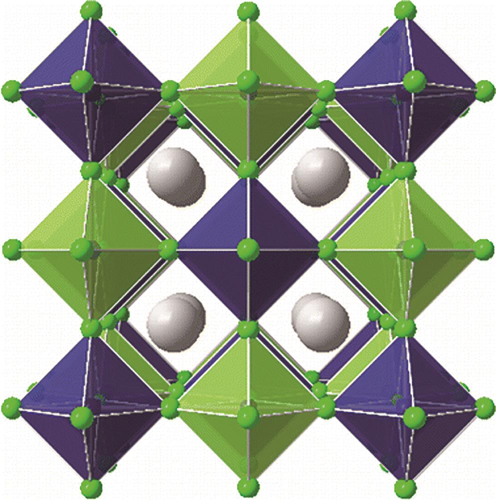
    Refined crystal structure of Cs2AgBiBr6 (Cs+ ions are shown as big gray spheres, bromine ions as other small spheres, while Ag and Bi centered octahedra are shown as dark and light colour polyhedra, respectively)[37]
    Fig. 1. Refined crystal structure of Cs2AgBiBr6 (Cs+ ions are shown as big gray spheres, bromine ions as other small spheres, while Ag and Bi centered octahedra are shown as dark and light colour polyhedra, respectively)[37]
    Current density-voltage (J-V) curves of a solar cell[66]
    Fig. 2. Current density-voltage (J-V) curves of a solar cell[66]
    Schematic diagram of Cs2AgBiBr6 single crystal growth by hydrothermal reaction process[79]
    Fig. 3. Schematic diagram of Cs2AgBiBr6 single crystal growth by hydrothermal reaction process79
    Isostatic-pressing method to prepare Cs2AgBiBr6 wafers[80]. (a) Schematic illustration of isostatic-pressing process; (b) as-prepared Cs2AgBiBr6 wafers with tunable sizes and diameters are 5, 3, and 1 cm from left to right; (c) top-down SEM image of wafer; (d) cross-sectional SEM image of wafer and inset is a higher resolution image, demonstrating grain size is larger than 100 μm
    Fig. 4. Isostatic-pressing method to prepare Cs2AgBiBr6 wafers[80]. (a) Schematic illustration of isostatic-pressing process; (b) as-prepared Cs2AgBiBr6 wafers with tunable sizes and diameters are 5, 3, and 1 cm from left to right; (c) top-down SEM image of wafer; (d) cross-sectional SEM image of wafer and inset is a higher resolution image, demonstrating grain size is larger than 100 μm
    Fabrication and SEM images of Cs2AgBiBr6 film[88]. (a) Image of Cs2AgBiBr6 powder (left) and solution in DMSO (right); (b) film fabrication process diagram; SEM images of films obtained by (c) TA and (d) LPA process. Inset: film photograph with size of 25 mm×25 mm
    Fig. 5. Fabrication and SEM images of Cs2AgBiBr6 film[88]. (a) Image of Cs2AgBiBr6 powder (left) and solution in DMSO (right); (b) film fabrication process diagram; SEM images of films obtained by (c) TA and (d) LPA process. Inset: film photograph with size of 25 mm×25 mm
    Cs2AgBiBr6 films with cubic double perovskite structure fabricated by capillary-assisted dip-coating (CDC) method[92]
    Fig. 6. Cs2AgBiBr6 films with cubic double perovskite structure fabricated by capillary-assisted dip-coating (CDC) method[92]
    Scheme of sequential vapor deposition processing[46]
    Fig. 7. Scheme of sequential vapor deposition processing[46]
    Schematic of Cs2AgBiBr6 film preparation using single source vapor deposition method[97]
    Fig. 8. Schematic of Cs2AgBiBr6 film preparation using single source vapor deposition method[97]
    Synthesis of Cs2AgBiX6 nanocrystals[99]
    Fig. 9. Synthesis of Cs2AgBiX6 nanocrystals[99]
    Thermal injection and anti-solvent recrystallization for colloidal synthesis of Cs2AgBiBr6 double perovskite NCs[47]
    Fig. 10. Thermal injection and anti-solvent recrystallization for colloidal synthesis of Cs2AgBiBr6 double perovskite NCs[47]
    Structure of solar cell[1]. (a) Schematic of n-i-p architecture; (b) schematic of p-i-n architecture
    Fig. 11. Structure of solar cell[1]. (a) Schematic of n-i-p architecture; (b) schematic of p-i-n architecture
    Current density-voltage (J-V) curves of forward and reverse scan directions[45]
    Fig. 12. Current density-voltage (J-V) curves of forward and reverse scan directions[45]
    Current density-voltage (J-V) curves of forward and reverse scans directions after adding anti-solvent[105]
    Fig. 13. Current density-voltage (J-V) curves of forward and reverse scans directions after adding anti-solvent[105]
    Band gap evolution of Cs2AgBiBr6 crystal at high pressure and representative optical micrographs[117]
    Fig. 14. Band gap evolution of Cs2AgBiBr6 crystal at high pressure and representative optical micrographs[117]
    Current density-voltage (J-V) curves of forward (broken lines) and reverse (solid lines) scan directions[48]
    Fig. 15. Current density-voltage (J-V) curves of forward (broken lines) and reverse (solid lines) scan directions[48]
    Device configurationFabrication methodJsc /(mA·cm-2Voc /VFFPCE /%Ref.
    ITO/c-TiO2/Cs2AgBiBr6/spiro-OMeTAD/AuSpin coating1.551.060.741.22106
    FTO/c-TiO2/m-TiO2/Cs2AgBiBr6/Spiro/AuSpin coating2.101.020.641.40107
    FTO/c-TiO2/C60/Cs2AgBiBr6/PCPDTBT/AuSpin coating2.251.010.691.57108
    FTO/c-TiO2/m-TiO2/Cs2AgBiBr6/spiro-OMeTAD/AgSpin coating3.221.020.692.2848
    FTO/c-TiO2/m-TiO2/Cs2AgBiBr6/spiro-OMeTAD/AuSpin coating3.930.980.632.4383
    FTO/c-TiO2/Cs2AgBiBr6/spiro-OMeTAD/MoO3/AgSpin coating3.821.010.652.51103
    FTO/c-TiO2/m-TiO2/Li+-Cs2AgBiBr6/CarbonSpin coating3.151.120.692.57109
    ITO/SnO2/Cs2AgBiBr6/Zn-chlorophyll/AgSpin coating3.820.990.732.79110
    FTO/Ti3C2Tx/TiO2/Cs2AgBiBr6/spiro-OMeTAD/MoO3/AgSpin coating4.140.960.702.81111
    FTO/c-TiO2/m-TiO2/Cs2AgBiBr6/N719/spiro-OMeTAD/AgSpin coating5.131.060.522.84112
    FTO/c-TiO2/m-TiO2/C-Ch1/Cs2AgBiBr6/spiro-OMeTAD/AgSpin coating4.091.040.733.1148
    FTO/SnO2/Cs2AgBiBr6/P3HT/AuSpin coating-low pressure1.781.040.781.4490
    ITO/SnO2/Cs2AgBiBr6/Spiro-OMeTAD/MoO3/ITOSpin coating-low pressure2.200.970.741.56113
    ITO/SnO2/Cs2AgBiBr6/Spiro-OMeTAD/MoO3/AgSpin coating-low pressure2.481.080.762.05113
    FTO/c-TiO2/Cs2AgBiBr6/spiro-OMeTAD/AgSingle-source vapor deposition1.240.870.650.7097
    FTO/c-TiO2/Cs2AgBiBr6/P3HT/AuSequential vapor deposition1.791.120.681.3746
    FTO/c-TiO2/m-TiO2/Cs2AgBiBr6/Spiro-OMeTAD/AuSpin coating-antisolvent2.450.640.570.9065
    ITO/SnO2/Cs2AgBiBr6/spiro-OMeTAD/AuSpin coating-antisolvent1.690.900.741.11105
    FTO/TiO2/Cs2AgBiBr6/P3HT/AuSpin coating-antisolvent1.481.050.711.11104
    FTO/c-TiO2/m-TiO2/Cs2AgBiBr6/PTAA/AuSpin coating-antisolvent1.841.020.671.2665
    ITO/Cu-NiO/Cs2AgBiBr6/C60/BCP/AgSpin coating-antisolvent3.191.010.692.2345
    Table 1. Comparison of structure and performance of Cs2AgBiBr6 based lead-free perovskite solar cells
    Qi Han, He Liu, Fengyun Guo, Yong Zhang. Research Progress on Cs2AgBiBr6 Halide Double-Perovskite Solar Cells[J]. Laser & Optoelectronics Progress, 2023, 60(7): 0700004
    Download Citation