• Chinese Optics Letters
  • Vol. 22, Issue 1, 012501 (2024)
Tao Xun1、2、*, Xinyue Niu1, Langning Wang1、2、**, Bin Zhang1、2, Jinmei Yao1、2, Yimu Yu1、2, Hanwu Yang1、2, Jing Hou1、2, Jinliang Liu1、2, and Jiande Zhang1、2
Author Affiliations
  • 1College of Advanced Interdisciplinary Studies, National University of Defense Technology, Changsha 410073, China
  • 2Nanhu Laser Laboratory, National University of Defense Technology, Changsha 410073, China
  • show less
    DOI: 10.3788/COL202422.012501 Cite this Article Set citation alerts
    Tao Xun, Xinyue Niu, Langning Wang, Bin Zhang, Jinmei Yao, Yimu Yu, Hanwu Yang, Jing Hou, Jinliang Liu, Jiande Zhang. Recent progress of parameter-adjustable high-power photonic microwave generation based on wide-bandgap photoconductive semiconductors[J]. Chinese Optics Letters, 2024, 22(1): 012501 Copy Citation Text show less
    Different types of microwave sources.
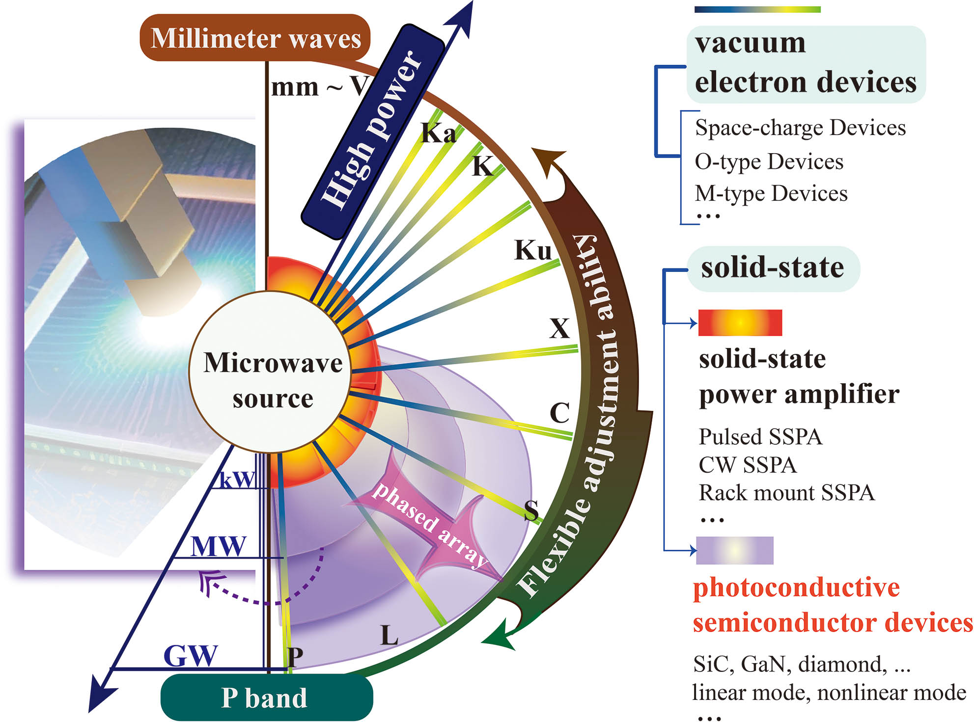
    Fig. 1. Different types of microwave sources.
    Schematic diagram of the principle of photoconductive microwave generation using wide-bandgap semiconductors.
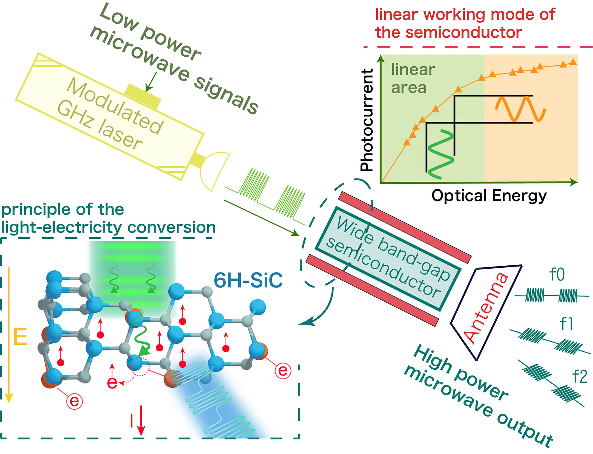
    Fig. 2. Schematic diagram of the principle of photoconductive microwave generation using wide-bandgap semiconductors.
    Equivalent circuit model of the device[45].
    Fig. 3. Equivalent circuit model of the device[45].
    Framework diagram of the transient photocurrent model of a 4H-SiC PCSD[48].
    Fig. 4. Framework diagram of the transient photocurrent model of a 4H-SiC PCSD[48].
    System architecture of the burst-mode-operation pulse laser, including the schematic diagram of the three-stage all-fiber amplifier[49] and the second-harmonic generation (SHG) system.
    Fig. 5. System architecture of the burst-mode-operation pulse laser, including the schematic diagram of the three-stage all-fiber amplifier[49] and the second-harmonic generation (SHG) system.
    Typical structure of a 6H-SiC device.
    Fig. 6. Typical structure of a 6H-SiC device.
    (a) Optimization of the optical coupling structure. (b), (c) Comparison of the outputs of systems with and without optical coupling[63].
    Fig. 7. (a) Optimization of the optical coupling structure. (b), (c) Comparison of the outputs of systems with and without optical coupling[63].
    (a) Experimental setup of the frequency-adjustable HPM generator based on a linear 6H-SiC PCSD, including (b) the integrated device and (c) the test circuit.
    Fig. 8. (a) Experimental setup of the frequency-adjustable HPM generator based on a linear 6H-SiC PCSD, including (b) the integrated device and (c) the test circuit.
    Experimental results of output waveforms of the SiC device with the 1064-nm pulse laser. (a) The output waveform at a modulated frequency of 1 GHz. (b) The typical normalized spectra of output waveforms with modulated frequencies ranging from 0.5 GHz to 2.5 GHz.
    Fig. 9. Experimental results of output waveforms of the SiC device with the 1064-nm pulse laser. (a) The output waveform at a modulated frequency of 1 GHz. (b) The typical normalized spectra of output waveforms with modulated frequencies ranging from 0.5 GHz to 2.5 GHz.
    (a) Breakdown process of the device, (b) optimized electrode structure with the double-sided AZO, and (c) effect of the optimized electrode structure on the lifetime and efficiency[66].
    Fig. 10. (a) Breakdown process of the device, (b) optimized electrode structure with the double-sided AZO, and (c) effect of the optimized electrode structure on the lifetime and efficiency[66].
    Key steps to achieve higher power and higher frequency output.
    Fig. 11. Key steps to achieve higher power and higher frequency output.
    Properties4H-SiCGaN
    Bandgap (eV)3.263.42
    Breakdown field (MV/cm)2.2–2.83.0
    Saturated electron velocity (107 cm/s)2.22.5
    Electron mobility [cm2/(V · s)]1020–12001500
    Dark resistivity (Ω · cm)1010–1012105–108
    Density (g/cm3)3.26.1
    Thermal conductivity [W/(cm · K)]4.51.3
    Table 1. Comparison of the 4H-SiC and GaN Properties
    SymbolDefinitionSymbolDefinition
    VD/VN/VAConcentration of V in donor/neutral/acceptor stateS0Substrate area
    Gij/RijCarrier generation/recombination rate in each channeldSubstrate thickness
    σijOptical absorption cross section in each channelμn0/μnLow field/strong field mobility
    αEPhoto-generated carrier generation coefficientvsatSaturated carrier drift velocity
    AAbsorption coefficientβFitting coefficient
    ηQuantum efficiencyETransient electric field
    PIncident light powernij/pijElectron/hole concentration of impurity energy level ionization
    Table 2. Definitions of the Physical Quantities
    SymbolDefinitionMeasured/calculated valueUnit
    RloadLoad resistance (port impedance)50Ω
    k1Attenuation factor of the attenuator40dB
    k2Attenuation factor of the directional coupler40dB
    VtestPeak-to-peak voltage detected by the oscilloscope1.65V
    VP-PPeak-to-peak voltage of the actual output signal16.5kV
    PoutOutput power1.36MW
    Table 3. Definitions and Measured Values of the Physical Quantities
    Tao Xun, Xinyue Niu, Langning Wang, Bin Zhang, Jinmei Yao, Yimu Yu, Hanwu Yang, Jing Hou, Jinliang Liu, Jiande Zhang. Recent progress of parameter-adjustable high-power photonic microwave generation based on wide-bandgap photoconductive semiconductors[J]. Chinese Optics Letters, 2024, 22(1): 012501
    Download Citation