
Tao Xun, Xinyue Niu, Langning Wang, Bin Zhang, Jinmei Yao, Yimu Yu, Hanwu Yang, Jing Hou, Jinliang Liu, Jiande Zhang. Recent progress of parameter-adjustable high-power photonic microwave generation based on wide-bandgap photoconductive semiconductors[J]. Chinese Optics Letters, 2024, 22(1): 012501
- Chinese Optics Letters
- Vol. 22, Issue 1, 012501 (2024)
Abstract
Keywords
1. Introduction
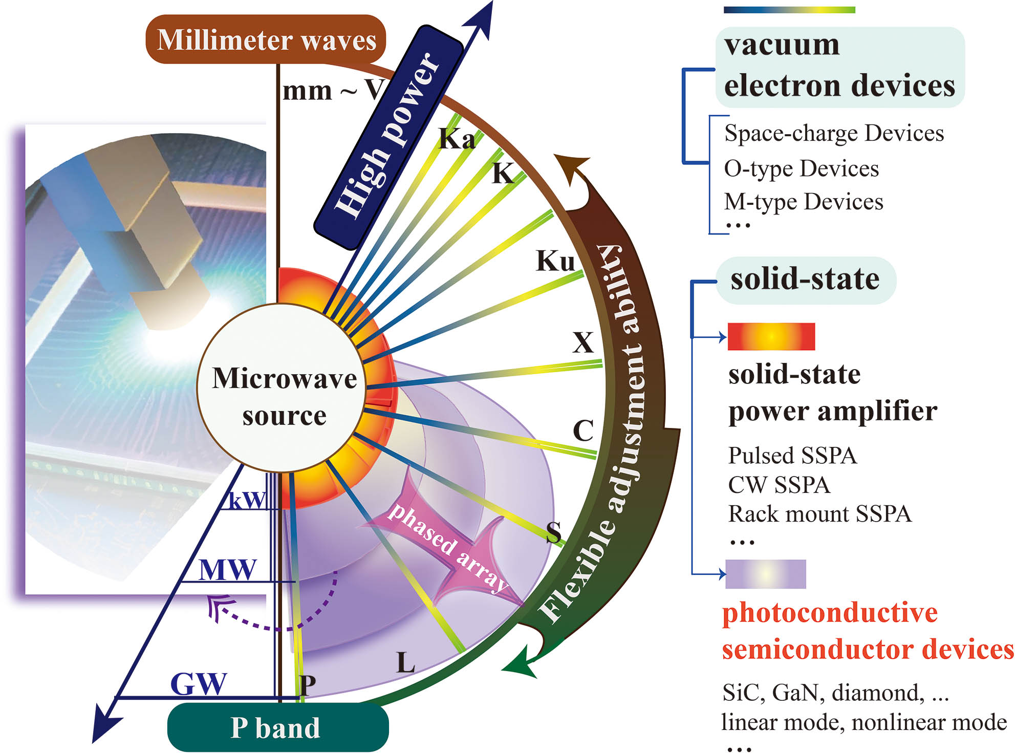
High-power microwave (HPM) sources have essential applications in directed energy weapons, pulsed and continuous wave radars, particle accelerators, industrial microwave heaters, and plasma generators[1–4]. HPMs can be generated in two ways, vacuum electronic devices and solid-state devices, both of which have their characteristics and advantages. The schematic diagram of various microwave sources and their output parameters is illustrated in Fig. 1, where the radial coverage length represents the output power level, and the circumferential coverage range represents the frequency tuning range of the device.
![]()
Figure 1.Different types of microwave sources.
Vacuum electronic devices have apparent advantages in high-power applications, with a peak power up to the GW level and a frequency up to the Ka-band[5]. However, microwaves generated by traditional relativistic electron devices generally operate with fixed output parameters, which poses difficulties for target adaptation and integration applications[6,7]. With the continuous development of semiconductor technology, solid-state microwave technology has attracted more attention, mainly including solid-state power amplifier technology and photoconductive radio frequency (RF)/microwave technology[8].
Based on field effect transistors, solid-state power amplifiers can realize high-frequency output in the mm band and have the advantages of miniaturization, multifunctionality, and suitability for multi-platform loading. However, the single-chip peak power is low (), and higher output is generally achieved by multi-channel synthesis[9,10]. The complexity and cost of a GW-level system will face significant challenges.
Sign up for Chinese Optics Letters TOC. Get the latest issue of Chinese Optics Letters delivered right to you!Sign up now
Photoconductive RF/microwave technology based on photoconductive semiconductor devices (PCSDs) integrates wide bandgap semiconductor technology, high-repetition-rate pulsed laser technology, and pulsed power technology[1,2,11–13]. By fully using the material advantages of wide-bandgap semiconductors, whose bandgap energy and breakdown field exceed 3 eV and 2 MV/m, respectively, the peak power of a single-channel output of the PCSDs, in theory, can reach a high level.
PCSDs have linear and nonlinear operation modes, and their working mechanisms are quite different. A nonlinear PCSD is switched on by a laser with lower optical excitation energy at the nJ level[14–16]. The semiconductor initially produces a few carriers, which are then magnified by a field-avalanche process called “lock-on”[17,18]. The current persists after the laser pulses activate the PCSDs and fades as the electric field weakens. The pulse widths of a nonlinear PCSD are much longer than the pulse widths of the incident lights. The rise and fall times of the outputs are usually hundreds of picoseconds, which define its central frequency (usually )[14–19] and make the output microwave parameters difficult to modify. Unlike nonlinear devices, such as GaAs photoconductive switches that aim for larger on-state currents, linear photoconductive devices pursue more of a balance between high power capacity and wide tuning range. Linear PCSDs usually show light-controlled resistance with a short recombination lifetime of ∼100 ps[20].
The principle of photoconductive microwave generation using linear-mode wide-bandgap semiconductors SiC is shown in Fig. 2. The V-doped SiC can be excited by a sub-bandgap light at a wavelength of 1064 nm (1.16 eV) due to the presence of the V acceptor level being at 0.7 eV below the conduction band[21]. The linear working mode of the SiC PCSDs makes the output waveform links highly consistent with the modulated laser waveform. Therefore, it acts as a microwave power amplifier that can respond to high-frequency (GHz) modulated light sources to produce tunable high-power RFs. Its low jitter feature[22,23] gives it the potential to achieve GW-level output by array synthesis. Moreover, the spatial current distribution generated in the photoconductive semiconductor switches (PCSS) operating in the linear mode is more uniform, which benefits the long-life operation of the PCSS. The HPM generating based on PCSDs is brand new territory in parameter-adjustable solid-state high-power microwave technology.
![]()
Figure 2.Schematic diagram of the principle of photoconductive microwave generation using wide-bandgap semiconductors.
SiC and GaN are two most typical materials used in wide bandgap semiconductors. The former is an indirect bandgap material and can only work in linear mode. While the latter is an direct bandgap material and works in linear mode under low voltage and in nonlinear mode under high voltage. The electron mobility of GaN is relatively high, making it a potential candidate for ultra-fast response applications[24,25]. Significant work is presently being done to improve the quality of GaN. However, high quality bulk GaN is still not currently widely available[26]. In contrast, SiC is widely used in high-power and high-temperature scenarios because of its advantage of high thermal conductivity, which is significantly higher than that of GaN. More importantly, compared with GaN, the production process of SiC is more mature. Thus, SiC can fully demonstrate the advantages of a wide bandgap and a high breakdown field[11,27–32]. The detailed comparison of the two materials is shown in the Table 1.
| Properties | 4H-SiC | GaN |
|---|---|---|
| Bandgap (eV) | 3.26 | 3.42 |
| Breakdown field (MV/cm) | 2.2–2.8 | 3.0 |
| Saturated electron velocity (107 cm/s) | 2.2 | 2.5 |
| Electron mobility [cm2/(V · s)] | 1020–1200 | 1500 |
| Dark resistivity (Ω · cm) | 1010–1012 | 105–108 |
| Density (g/cm3) | 3.2 | 6.1 |
| Thermal conductivity [W/(cm · K)] | 4.5 | 1.3 |
Table 1. Comparison of the 4H-SiC and GaN Properties
In recent years, researchers have conducted many studies on device failure mechanisms[33] and enhanced device lifetimes using techniques, such as plating[34,35], changing electrode shapes, and modifying triggering methods[36,37], which offer valuable references for improving device lifetimes. In the future, the power of combining those devices will be a vital pathway for finding practical applications for optical switching devices[38–40]. To meet the needs of phased arrays, except for the characteristic of being parameter-adjustable[41,42], lasers also must be capable of multi-channel topologies[43,44], which will draw extensive attention from researchers to inter-channel delay tuning.
This paper mainly introduces the latest research progress of high-power photonic microwave generation based on V-doped SiC photoconductive semiconductors. In order to clarify the operating mechanism, two equivalent models of the linear-mode PCSDs are introduced in Section 2. Then, in Section 3, progress in the high-power microwave generation based on PCSDs is shown, including the pulse laser, the device fabrication and processing, and the verification experiments. Next in Section 4, the damage mechanism of the PCSDs is shown and analyzed. Finally, Section 5 contains the summary of this paper, the future challenges, and the development methods of the PCSDs.
2. Equivalent Models for the Linear-Mode PCSDs
The resistance of the device is an important factor that determines the output parameters, and it is significant to construct an equivalent model that includes this resistance. There are two types of models used to obtain the device’s on-resistance: the macroscopic (circuit) models and the microscopic models. They are described and contrasted in the following paragraphs.
Figure 3 shows the macroscopic (circuit) model[45–47] of a typical PCSD. The carrier lifetime is determined by the time constant, which is obtained by the convolution of the resistor-capacitor (RC) parallel circuits. Next, the SiC resistivity and output voltage, in turn, are calculated by Eqs. (1) and (2), respectively, where is the light absorption coefficient related to the coupling method of the incident light; is the transient power of the incident light; and is the circuit load, whose resistance is equal to the input impedance of actual applications such as wide-band antennas. The physical meanings of the other parameters are shown in Table 2. The RF modulation and amplification are realized by the inverse proportion relationship between light intensity and resistance,
| Symbol | Definition | Symbol | Definition |
|---|---|---|---|
| VD/VN/VA | Concentration of V in donor/neutral/acceptor state | S0 | Substrate area |
| Gij/Rij | Carrier generation/recombination rate in each channel | d | Substrate thickness |
| σij | Optical absorption cross section in each channel | μn0/μn | Low field/strong field mobility |
| αE | Photo-generated carrier generation coefficient | vsat | Saturated carrier drift velocity |
| A | Absorption coefficient | β | Fitting coefficient |
| η | Quantum efficiency | E | Transient electric field |
| P | Incident light power | nij/pij | Electron/hole concentration of impurity energy level ionization |
Table 2. Definitions of the Physical Quantities
![]()
Figure 3.Equivalent circuit model of the device[
Due to many light absorption channels that are introduced by energy levels of impurities, and the phenomenon that some light absorption channels absorb photons while not generating carriers, it is not easy to calculate the contribution of each energy level. Therefore, building a transient photocurrent model with different light absorption cross sections is vital for our research. This can act as a bridge between the doping mechanism and the characteristics of the output waveform. The microscopic calculation model is shown in Fig. 4.
![]()
Figure 4.Framework diagram of the transient photocurrent model of a 4H-SiC PCSD[
A transient photocurrent model of a 4H-SiC substrate excited with a 532-nm light was built in MATLAB[48], which explains the influence process of the critical factors on the output current of the PCSDs, such as impurity energy levels and their doping concentrations. The parameters in the framework are solved in the following order. First, the equilibrium carrier concentration and impurity ionization concentration are solved under the steady state. Second, the pathways of the carrier generation are defined according to the wavelength of the incident light and the energy levels of the material. Then, the transient carrier concentration is calculated through ordinary differential equations containing carrier generation terms and recombination terms. Finally, the transient photocurrent is calculated according to the electron mobility and carrier concentration models.
As shown in Fig. 4, increasing the density of the doped impurities extends the carrier lifetime, causing a tail in the waveform. When the tail is long, the continuous output wave will contain an additional direct current (DC) component, which consumes electrical energy but cannot radiate as microwaves, reducing the effective amplitude of the output voltage. On the other hand, reducing the doping concentration of impurities will reduce the carrier lifetime, and thus improve the response speed of the device, but this will also reduce the output peak power. Therefore, the contradiction of doping concentration will be encountered in the actual design, which leads to the need for different doping schemes in different applications. Although this calculation seems more complicated than the former, optimizing the doping mechanism by using the microscopic model can provide precise theoretical guidance and significantly save research costs.
3. Progress in the High-power Output of PCSDs
3.1. Architecture of the modulated pulse laser
Figure 5 shows the system architecture of the burst-mode-operation pulsed laser[50–53]. The burst-mode laser has the characteristics of a continuously adjustable intra-burst repetition rate and high peak power[49]. The repetition and duration of the electrical pulse-driven narrow-band laser diode (LD) are set as 25 kHz and 100 ns, respectively. The duty cycle of the subpulse is 50%. The acoustic-optic modulator (AOM) with a high extinction ratio is employed to program the temporal pulse waveform to compensate for the envelope distortion induced by the gain saturation effect. Then, an electro-optical modulator (EOM) accompanied by an arbitrary waveform generator (AWG) modulates the laser pulse into burst-mode operation with a modulating frequency at the GHz level. Thus, a burst-mode seed laser with milliwatt-level average power is obtained by the combination of the AOM and the EOM.
![]()
Figure 5.System architecture of the burst-mode-operation pulse laser, including the schematic diagram of the three-stage all-fiber amplifier[
After that, the seed laser is amplified by a three-stage all-fiber amplifier. The first stage uses a highly -doped single-cladding polarization-maintaining (PM) fiber that is bi-directionally pumped by two 976-nm LDs through the WDMs. The second stage employs -doped double-cladding PM fiber that is pumped by a 976 nm multi-mode LD through a pump-signal combiner. Finally, the burst-mode laser enters the main amplifier. The main amplifier consists of a highly -doped double-cladding PM fiber that is pumped by a 976-nm multi-mode LD through a pump-signal combiner. Thus, the output optical peak power can reach the kW level. Then, we utilize the Pockel cell to descend the burst repetition rate to 100 Hz. The laser is further amplified by a multi-stage solid-state amplifier. Next, the 1064-nm laser is changed to a 532-nm laser by a second harmonic generation (SHG) system, including a lithium borate (LBO) frequency-doubling crystal. Its maximum single pulse energy can reach the 10 mJ level.
3.2. Progress in device fabrication and processing
Obtaining quality doped single crystals is the basis for carrying out this project. The preparation and packaging technology of wide-bandgap device-specific crystals has been mastered by our laboratory. In many verification experiments, by measuring the macro electrical parameters of the output waveform, the core indicators, such as breakdown voltage, response rate, and photoconductivity of the samples, were obtained, and important parameters such as defect energy level and doping concentration were calculated. The crystal preparation process makes it possible to explore the balance of efficient excitation (increasing quantum efficiency) and efficient compensation (reducing carrier lifetime). Experiments were carried out based on the guidance of theoretical and simulation models, and the crystals’ design basis that met the requirements was obtained[54].
The optical penetration depth is determined by the optical absorption coefficient and the impurity concentration of the semiconductor material at a given wavelength. For linear extrinsic PCSDs, the absorption depth of the substrate is large. Thus, those PCSDs are usually constructed in a vertical structure. Due to the combination of coaxial structures and vertical devices, vertical PCSDs have significantly higher power capacity compared to planar ones[20,21] and can now work continuously under bias voltages exceeding 20 kV. Lateral devices have wider tuning ranges than vertical ones, owing to their lower parasitic capacitances and inductances[22,25].
The switching current penetrates the inside of the semiconductor, and the maximum working voltage is limited by the field enhancement of the triple junction, which is higher than that of the planar structure and has a longer lifetime. By optimizing the structures of electrodes and packages, the distribution characteristics of the internal electric field can be improved, and the risk of a breakdown inside the package can be reduced. A packaging method for SiC devices is proposed, forming an overall packaging design and processing technology scheme. The problem of achieving the stable operation of a single device with 20 kV high power capacity has been solved through continuous research and optimization of the structure, the processing technology, and the device fabrication of vertical PCSDs[55]. Figure 6 shows the typical structure of a vertical PCSD.
![]()
Figure 6.Typical structure of a 6H-SiC device.
Linear intrinsic devices are usually constructed in a lateral structure. The switching current is concentrated on the surface of the semiconductor, and the maximum working voltage is limited by surface flashover. Since high-resistance SiC substrate is used as the material for device fabrication, the design of the ohmic electrode structure is another critical research content of the device design[56–59]. Using SiC epitaxial technology, a 1-µm-thick heavily doped n+ epitaxial layer is epitaxially grown on a high-resistance SiC substrate, and ohmic contact electrodes are fabricated on this epitaxial layer. This scheme can effectively avoid adverse factors such as lattice damage caused by ion implantation to SiC materials. The technologies of planar electrode fabrication mainly include coating, lithography, etching, processing metal electrodes, stripping, and thinning.[60–62].
The ultimate purpose of designing an optical coupling structure is to make the PCSDs utilize as much light energy as possible, that is, to achieve efficient photoelectric conversion, which mainly has two indicators[63–65]. One is the gain of the light energy. By constructing a total internal reflection cavity, thus increasing the optical transmission path, the light absorption of the substrate is increased. The other is the homogenization ability to the energy distribution of the incident laser, which reduces the probability of device damage caused by excessive photocurrent density. For this purpose, we used various optical lenses in the design structure. We selected and optimized a total internal reflection light-capture structure with a focusing lens, as shown at the top of Fig. 7(a).
![]()
Figure 7.(a) Optimization of the optical coupling structure. (b), (c) Comparison of the outputs of systems with and without optical coupling[
The simulation model was built, and the light flux distribution map was obtained in Tracepro. After adding the optical coupling structure, the light flux is increased to 2.45 times the original, and the energy distribution uniformity of the light spot is significantly improved. Figure 7(b) shows the transient response current waveforms before and after the improvement of the optical coupling structure under the conditions of bias voltage 6 kV and pulse light energy 0.234 mJ, proving that the waveform distortion introduced by the proposed structure can be ignored, and the light power is increased to twice of the original. The minimum on-resistance before and after optimization under different electric field strengths and light energies is compared in Fig. 7(c). The average value of the reduced ratio of minimum on-resistance is 2.58, which is consistent with the light power increased ratio of 2.45 in the simulation. This structure increases the photoelectric gain from 2 dB to 6 dB, reduces the demand for light power, and is conducive to system compactness and integrated applications.
3.3. Verification experiments of PCSDs
In this subsection, through experiments, we verified that the all-solid-state optically controlled microwave source has the characteristics of continuous tunability of the central frequency in the P and L microwave bands, and the peak power of the RF output can reach the MW (megawatt) level. The experimental setup is shown in Fig. 8(a). The laser was coupled into the fiber through the focusing lens and the three-dimensional adjustment bracket and illuminated the photoconductive semiconductor.
![]()
Figure 8.(a) Experimental setup of the frequency-adjustable HPM generator based on a linear 6H-SiC PCSD, including (b) the integrated device and (c) the test circuit.
The PCSD integrated structure can be divided into a SiC substrate with electrodes, as shown in Fig. 7(a), and a coaxial structure, as shown in Fig. 8(b). A high voltage DC (HVDC) system charged the capacitors around the axis, equivalent to a voltage source with a 30 kV power supply capacity. The 1064-nm laser used in the experiment had a repetition frequency of 100 Hz, a pulse envelope width of 100 ns, and an energy of 25 mJ per pulse. The output signal was transmitted to a sampling oscilloscope with a bandwidth of 4 GHz via a 40 dB directional coupler and a 4 GHz/50 Ω/40 dB attenuator. The test circuit is shown in Fig. 8(c). The meanings and measured values of the physical quantities are shown in Table 3.
| Symbol | Definition | Measured/calculated value | Unit |
|---|---|---|---|
| Rload | Load resistance (port impedance) | 50 | Ω |
| k1 | Attenuation factor of the attenuator | 40 | dB |
| k2 | Attenuation factor of the directional coupler | 40 | dB |
| Vtest | Peak-to-peak voltage detected by the oscilloscope | 1.65 | V |
| VP-P | Peak-to-peak voltage of the actual output signal | 16.5 | kV |
| Pout | Output power | 1.36 | MW |
Table 3. Definitions and Measured Values of the Physical Quantities
Because the test signal passed through the coaxial-waveguide directional coupler and wide-band attenuator, it is necessary to calibrate the two measuring instruments before the experiment. This has important significance and influence on the accuracy of the experimental results. After calibration, the total attenuation factor of the test circuit () was obtained, and the actual output voltage was calculated according to Eq. (3). The output power, which was delivered to the antenna or other loads, was calculated according to Eq. (4). The meanings and measured values of the physical quantities in the equations are shown in Table 2,
As shown in Fig. 9, when output frequencies range from 0.5 to 2.5 GHz, the waveforms of the photocurrents are identical to that of the pulsed lasers, and the output signals are narrow-spectrum signals, indicating that the vanadium-compensated semi-insulating (VCSI) SiC devices indeed have a fast and linear response. Thus, it was confirmed by experiments that the SiC photoconductive system could generate frequency-adjustable, megawatt-class microwave output signals, and the output frequency was continuously adjustable from the P band to the L band. The response frequency can be further improved by optimizing the doping mechanism of VCSI SiC or reducing the interstage capacitance of the device.
![]()
Figure 9.Experimental results of output waveforms of the SiC device with the 1064-nm pulse laser. (a) The output waveform at a modulated frequency of 1 GHz. (b) The typical normalized spectra of output waveforms with modulated frequencies ranging from 0.5 GHz to 2.5 GHz.
4. Damage Mechanism of PCSDs
The main failure mechanisms of the device can be divided into the thermal damage caused by the laser and the avalanche breakdown caused by the bias voltage. It has been experimentally verified that the latter is the dominant factor that affects the device’s lifetime. Under dark-state conditions, the field distribution is relatively uniform, and the carriers at the end of the anode are broken down by avalanche multiplication. The experimental device has a dark-state breakdown threshold of 22 kV. Under conduction conditions, the illuminated area can be regarded as a reduced inter-level distance. Hence, the field strength in the anode light transmission area is much greater than in other areas, causing more severe damage to the device. When the device electrodes are damaged, although the field distribution changes little, the current distribution changes considerably, resulting in thermal damage to the device.
The process of device breakdown is inferred from a large number of experimental phenomena, as shown in Fig. 10(a). First, the laser irradiates the device surface and interacts with the transparent electrode. The transparent electrode absorbs the laser energy and deforms and changes phase. Second, after the deformation of the transparent electrode reaches a certain degree, the transmitted laser converges into multiple small-sized self-focusing beams behind it, causing micro-damage points on the Ag mirror electrode. Third, with the accumulation of heat from the incident and reflected light, the transparent electrode gradually melts and ablates. Part of the laser pulse directly irradiates the SiC crystal surface. Therefore, field enhancement points will be generated near the contact point of the SiC crystal, the transparent electrode, and the air, which will cause a significant increase in current density. The damage will first occur at this three-junction point, and then a pre-breakdown channel will be formed, finally leading to device breakdown failure. Figure 10(b) shows the optimized electrode structure, which uses a configuration with double-sided AZO transparent electrodes to homogenize the light spot, reduce the field strength, and increase the optical path[67]. As shown in Fig. 10(c), under the experimental conditions of a repetition frequency of 100 Hz, a bias voltage of 8 kV, and an incident light energy of 8 mJ, compared with the unoptimized devices, the lifetimes of the PCSDs are increased by more than ten times. The output efficiencies are increased by about 20%, achieving an output of 100 A-level current conditions for more than 10 minutes[66].
![]()
Figure 10.(a) Breakdown process of the device, (b) optimized electrode structure with the double-sided AZO, and (c) effect of the optimized electrode structure on the lifetime and efficiency[
5. Summary
This paper introduces the latest research progress in wide-parameter photonic microwave generator devices based on an optically controlled wide bandgap semiconductor. The latest research results are given from multiple aspects, including the basic principle, pressure-resistant packaging, high-frequency response, optoelectronic coupling, and typical test results of the PCSDs. The vertical PCSDs have continuous tunable central frequencies from the P band to the L band. Its peak power of single-channel output can reach the MW level. In the future, we will continue to expand the frequency tuning range of vertical devices. Furthermore, we have realized an operating lifetime over 10 minutes under 100 A-level current conditions for vertical devices. In the future, we plan to change electrode shapes and modify triggering methods to enhance device lifetimes. Other aspects worth exploring include optical coupling structures, RF output structures, and phased array designs. Their optimization can further improve device efficiency, so continued efforts are still necessary. Figure 11 shows the key steps for improving the power capacity and output bandwidth of photoconductive microwave generation systems. This provides a reference for applying PCSDs in high-power microwave sources.
![]()
Figure 11.Key steps to achieve higher power and higher frequency output.
Currently, PCSD development is faced with the challenge of realizing efficient photoelectric conversion and high-speed compensation, that is, high power and fast response at the same time. The single-channel output of photoconductive devices is limited by the devices’ pressure-bearing capacity and the waveform distortion under strong light conditions. Therefore, while continuously improving the single-channel power capacity or response bandwidth, the development of PCSDs for high-power applications will inevitably require multi-channel power combining.
The combination of microwave photonics technology and phased arrays can also breakthrough the instantaneous bandwidth limitation under wide-band and wide-angle conditions. The optical true time delay (OTTD) phased array antenna (PAA) can avoid beam squint of the array, which significantly reduces the broadband power synthesis loss. The only factor that affects the synthesis efficiency is the phase (time delay) synchronicity of the array elements. The delay accuracy of optical signals can reach fs levels, indicating that photoconductive microwave phased array systems have great potential in high-precision power synthesis. The most important step is the combination of delay tuning techniques and high-power fields. Other problems that need attention are multi-channel signal jitter measurement and delay difference measurement, which provide the basis for delay adjustment.
References
[1] J. Seeds, K. J. Williams. Microwave photonics. J. Lightwave Technol., 24, 4628(2006).
[2] J. Capmany, D. Novak. Microwave photonics combines two worlds. Nat. Photon., 1, 319(2007).
[3] J. Yao. Arbitrary waveform generation. Nat. Photon., 4, 79(2010).
[6] D. L. Adamy. Introduction to Electronic Warfare Modeling and Simulation(2003).
[9] J. D. McKinney. Photonics illuminates the future of radar. Nature, 507, 310(2014).
[10] J. Benford, J. A. Swegle, E. Schamiloglu. High Power Microwaves(2015).
[24] M. E. Levinshtein, S. L. Rumyantsev, M. S. Shur. Properties of Advanced Semiconductor Materials: GaN, AlN, InN, BN, SiC, SiGe(2001).
[27] J. S. Sullivan. Wide bandgap extrinsic photoconductive switches(2013).

Set citation alerts for the article
Please enter your email address
© Copyright 2018-2021 | Chinese Laser Press. All Rights Reserved 沪ICP备15018463号-20