Abstract
In this work, high-efficiency AlN/GaN metal-insulator-semiconductor high electron mobility transistors (MIS-HEMTs) have been fabricated for millimeter wave applications. A 5-nm SiNx insulator is grown in-situ as the gate insulator by metal-organic chemical vapor deposition (MOCVD), contributing to remarkably suppressed gate leakage, interface state density and current collapse. The fabricated MIS-HEMTs exhibit a maximum drain current of 2.2 A/mm at VGS=2 V, an extrinsic peak Gm of 509 mS/mm, and a reverse Schottky gate leakage current of 4.7×10⁻⁶ A/mm when VGS = -30 V. Based on a 0.15 μm T-shaped gate technology, an fT of 98 GHz and fMAX of 165 GHz were obtained on the SiN/AlN/GaN MIS-HEMTs. Large signal measurement shows that, in a continuous-wave mode, the MIS-HEMTs deliver an output power density (Pout) of 2.3 W/mm associated with a power-added efficiency (PAE) of 45.2% at 40 GHz, and a Pout (PAE) of 5.2 W/mm (42.2%) when VDS was further increased to 15 V.Introduction
In recent years,high electron mobility transistors(HEMTs)based on GaN have attracted more attention,due to their high thermal conductivity,high breakdown voltage,and high-power density for millimeter-wave(mm-wave)power amplifiers. In an AlGaN/GaN HEMTs structure,the working voltage may reach 28 V or even higher[1][2],such high voltage will enhance the longitudinal electric field to increase the gate leakage[3]. Additionally,the internal electric field intensity will reach 106~107 V/cm when the 20~30 V is applied to drain bias,leading to current collapse,reduction of breakdown voltage,and increase in leakage[4]. In order to achieve high-performance GaN HEMT at low operating voltage,the energy-band theory is used to design new epitaxial structures to increase the electron gas density meanwhile preventing the gate from losing its control ability for the short T-gate. Therefore,the ultra-thin barrier layer technology has shown great advantages in ultra-high frequency and high power[5][6].
In millimeter-wave applications,the gate length is shrunk to deep-submicron size,and the transverse dimension of the device needs to be scaled down at the same proportion. To avoid the short channel effect,the material structure with an ultra-thin barrier layer is used to solve the aspect ratio of the gate. The issue primarily results from the much stronger spontaneous and piezoelectric polarization of AlN/GaN compared to AlGaN/GaN,leading to a much higher drain current in the HEMT channel,also allowing the use of a much thinner barrier layer. While along with the shrink of vertical device dimensions,increased gate leakage necessitates the use of a gate insulator[7-10].
AlN barrier has been shown highly sensitive to the air and vapor for oxidation,consequently,surface treatment and passivation techniques play a significant role in the surface state. To achieve a low gate leakage current,materials with a wide bandgap are necessary,such as SiO2 and Al2O3[7][9]. However,it is inevitable that these materials are deposited on the AlN surface when it is exposed to air,becoming contamination at the interfaces. On the other hand,in-situ deposition of SiNx is a promising way to realize proper interfaces,which guarantees the insensitivity of AlN surfaces to temperature change.
In this work,we demonstrated the AlN/ GaN MIS-HEMTs. By using in-situ SiNx insulator,a maximum drain current ID,max of 2.2 A/mm was obtained at VGS=2 V,it doubled ID,max of the AlGaN/GaN HEMTs under the same condition. Transconductance Gm,ext of 509 mS/mm are also achieved. Moreover,the OFF-state drain leakage,as well as gate leakage current in the HEMTs,was reduced by the low interface state between AlN barrier and insulator,contributing to a low Schottky gate leakage of 4.7×10⁻⁶ A/mm at VGS = -30 V and a low OFF-state drain leakage of 8.2×10⁻⁵ A/mm. Owing to the suppressed current collapse,when VDS = 8 V,a high output power density of 2.3 W/mm with peak power-added-efficiency(PAE)of 45.2%,and a power gain of 10.2 dB are achieved at 40 GHz in the continuous-wave(CW)mode.
1 Experiments
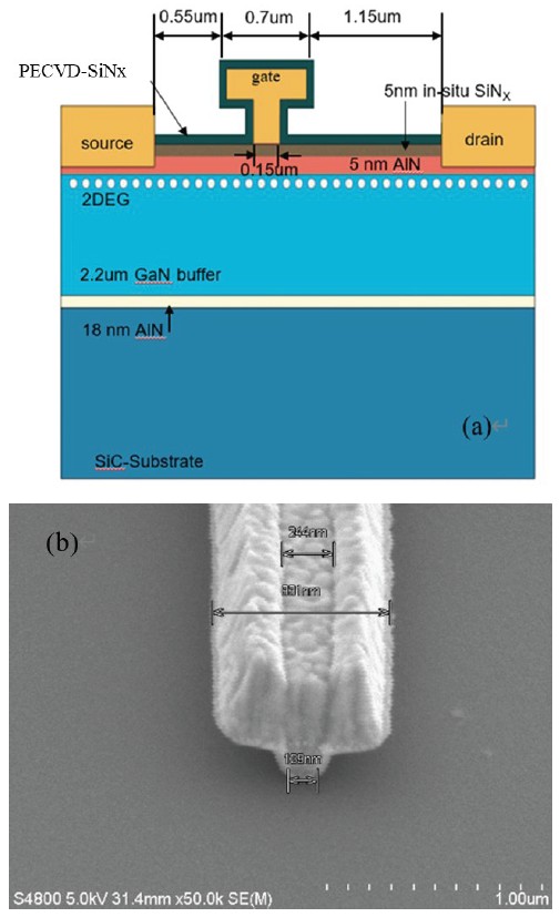
The schematic cross section of MIS-HEMTs is shown in Fig. 1(a). The AlN/GaN heterostructures in this study were grown on semi-insulating SiC substrates by metal-organic chemical vapor deposition(MOCVD),consisting of a Fe-doped GaN buffer layer,an unintentionally doped GaN channel layer,1 nm AlN spacer layer,a 5 nm AlN barrier layer,and 5 nm SiNx insulator layer. Device fabrication was started with source/drain ohmic contact formation by Ti/Al/Ni/Au stack,and subsequent rapid thermal annealed at 800 ℃ for 30 s in N2 atmosphere,to yield a contact resistance of 0.3 Ω·mm. Device isolation was then formed utilizing multiple-energy nitrogen ion implantation. A T-shaped gate was subsequently accomplished by electron beam lithography(EBL;model manufacturer)of UVIII/Al/PMMA resist stack. The width of the T-gate foot and head are 0.15 and 0.6 μm,respectively[2]. A Ni/Au metal layer was generated by e-beam evaporation(EVA450)on SiNx’s surface for the gate contact. Finally,the AlN/GaN HEMT devices were passivated with 60 nm stress-free SiNx grown by plasma-enhanced chemical vapor deposition(PECVD). The fabricated MIS-HEMTs have a source-drain distance(LSD)of 2.4 μm and a gate-drain distance(LGD)of 1.15 μm. An SEM picture of the T-gate is shown in Fig. 1(b).

Figure 1.(a) The schematic of epitaxial structure of AlN/GaN MIS-HEMTs, (b) the SEM of 0.15-μm T-gate
As a comparison,AlGaN/GaN HEMT devices are also developed,with the barrier and cap layers replaced with a 21-nm Al0.25Ga0.75N and a 3-nm GaN layers,respectively,as Ref.[16]. The gate recessed process,which differs from the AlN/GaN device’s,uses inductively coupled plasma(ICP)dry etching with chlorine-based plasmas of BCl3 and Cl2 to fabricate recessed-gate with a width of 0.8 μm and depth of 6 nm. Then the same T-shaped gates were fabricated on it. The remaining process steps are the same as for AlN/GaN devices.
2 Results and discussions
2.1 DC measurement
The fabricated devices yielded in this study exhibit a typical static characterization,as shown in Fig. 2(a). Due to the much stronger spontaneous and piezoelectric polarization of AlN/GaN,a maximum drain current of 2.2 A/mm at VGS=2 V was observed. The thickness of the in-situ SiNx cap layer is critical for highly scaled GaN devices to avoid gate leakage current contributing to a reverse density of 4.7×10⁻⁶ A/mm at VGS = -30 V,as shown in Fig. 2(b). The short-channel effect was effectively suppressed by the thin barrier,as shown by the transfer curves in Fig. 2(c),and the OFF-state drain leakage is merely 1.0×10⁻⁶ A/mm. Meanwhile the corresponding Gm,ext at VDS = 6 V is 509 mS/mm(Fig. 2(c)). Based on AlGaN barrier device,Gm,ext is 294 mS/mm and the OFF-state drain leakage is 8.2×10⁻⁵ A/mm under the same test condition(Fig. 2(d)).
Figure 2.Measured dc characteristics of devices (a) ID of both HEMTs and MIS-HEMTs versus VDS with VGS varied from -6 V to 2 V, (b) gate leakage of HEMTs and MIS-HEMTs with VGS swept to -30 V, (c) ID and extrinsic transconductance of MIS-HEMTs with VGS varied from -6 V to 2 V at VDS= 6 V, (d) ID and extrinsic transconductance of HEMTs with VGS varied from -6 V to 3 V at VDS= 6 V
2.2 The small-signal RF characteristics
The small-signal RF characteristics of the fabricated MIS-HEMTs were measured using a network analyzer in a frequency range from 100 MHz to 40 GHz. Values of current-gain cutoff frequency fT and unit-power-gain frequency fMAX,as shown in Fig. 4,were determined by 20 dB/dec line extrapolated from the small-signal current gain |h21|and maximum stable gain(MSG). At VDS=10 V,fT and fMAX are 98 GHz and 165 GHz,respectively(Fig. 3). It implies that in-situ SiNx technology effectively suppresses the RF-Gm collapse in mm-wave AlN/GaN HEMTs.
Figure 3.Small-signal characteristics of the fabricated AlN/GaN MIS-HEMTs at VDS = 10 V
Figure 4.f/T-dependent C-V characteristics of AlN/GaN MIS-HEMTs with (a) fm varying from 1 KHz to 1 MHz, (b) T increasing from -25 ℃ to 150 ℃ fm varying at 10 KHz and 20 KHz (c) Dit-ET mapping in AlN/GaN MIS-HEMTs
2.3 CV and pulse measurement
To determine the quality of in-situ SiNx,the capacitance-voltage(C-V)measurement was employed to realize interface trap density. The frequency/temperature dispersions of the second slope in C-V curve were analyzed[11-13],and the results are shown in Fig. 4. With fm varying from 1 KHz to 1 MHz(Fig. 4(a)),and T increasing from 25 ℃ to 150 ℃(Fig. 4(b)),the C-V characteristics of AlN/GaN MIS-HEMT exhibits a slight(∆V less than 0.05 V)dispersions in multi-f/T ac-CV characteristics,indicating low Dit and high interface quality in MIS-HEMT. Accordingly,Dit at the in-situ SiNx/AlN interface was mapped against ET[14-15]. From EC-0.58 eV to EC -0.29 eV,Dit falls between 3.4×10¹¹ and 1.1×1012 cm-2eV-1(Fig. 4(c)).
The low interface state density ensures the low dc-RF dispersion,the pulse I-V characteristic of the devices is shown in Fig. 5(a). The pulse period and width were set to 10 μs and 200 ns,respectively. The gate-lag effect under a quiescent bias of(VGSQ,VDSQ)=(-6 V,0 V)barely changes in the MIS-HEMTs. The drain-lag ratio under a quiescent bias of(VGSQ,VDSQ)=(-6 V,15 V)is pretty weak in the saturation region(collapse ratio:1.5%,Fig. 5(a)). It is probably due to the N in the SiNx rather than the AlN barrier that leads N vacancies creating a conducting channel through the AlN barrier,hence low annealing temperature and time. The in-situ SiNx impeded the formation of nitrogen deficiency and oxidation of bare AlN surface when conventional process of ohmic annealing at above 800 °C,and suppressed damage to the AlN barrier during the process of extra SiNX ex-situ passivation. The ultralow dispersion implies that in-situ SiNX effectively obstructed the bombardment of ion when the plasm was generated. As shown the pulsed transfer characteristics curves in Fig. 5(b),hysteresis is less than 100 mV after sweeping from -8 V to 0 V,indicating significant suppression of deep interface traps with in-situ insulator.
Figure 5.Pulsed I-V characteristics of (a) output characteristics measured at VGS = 0 V, (b) transfer characteristics measured at VDS = 10 V
2.4 Large-signal measurement
Figure. 6 depicts the large-signal power performance of the mm-wave AlN/GaN MIS-HEMTs,evaluated at 40 GHz in CW mode,in comparison with AlGaN/GaN HEMTs. The devices were biased at Class-AB condition with low operation voltage,VDS = 8 V,VDS = 10 V,and VDS = 15 V,respectively. Load and source impedance were optimized for the best PAE before the evaluation.
Figure 6.Large-signal measurements at 40 GHz in CW mode (a) VDS=8 V, AlN/GaN MIS-HEMTs measurement, (b) VDS=8 V, AlGaN/GaN HEMTs measurement, (c) VDS=10 V, AlN/GaN MIS-HEMTs measurement, (d) VDS=10 V, AlGaN/GaN HEMTs measurement, (e) VDS=15 V, AlN/GaN MIS-HEMTs large-signal measurement, (f) VDS=15 V, AlGaN/GaN HEMTs measurement
Owing to the enlarged current density and minimized forward gate leakage current of AlN/GaN MIS-HEMTs,a record high PAE of 45.2% is achieved at VDS = 8 V,and the corresponding output power density and associated gain are 2.3 W/mm and 10.8 dB gain. By contrast,the PAE,output power density,and gain of AlGaN/GaN HEMTs are merely 42.6%,1.2 W/mm,and 9.1 dB respectively. when VDS = 10 V,Pout of AlN/GaN MIS-HEMTs reached 3.3 W/mm while that of AlGaN/GaN HEMTs is 1.5 W/mm;when VDS = 15 V,Pout of AlN/GaN MIS-HEMTs increased to 5.2 W/mm while that of AlGaN/GaN HEMTs is 2.8 W/mm. In previous research using the AlGaN HEMTs structure,Pout of 5.1 W/mm can be only obtained under VDS over 25 V[16]. The high performance of AlN/GaN HEMTs is believed to attribute to the wide conduction band between AlN and GaN,as well as the high-quality SiNx/AlN interface.
At low voltage,the power density of AlN / GaN thin barrier MIS-HEMTs based on in-situ SiN growth is nearly double that of AlGaN barrier devices,making them promising for low voltage applications.
3 Conclusions
With in-situ SiNx technique on AlN/GaN epi-structure and T-gate process,high-performance MIS-HEMTs have been fabricated for low VDS applications at Ka-band. A high-quality SiNx/AlN interface has been obtained,which was verified by analyzing the frequency and temperature-dependent of the second slope in the C-V characteristics. Using 0.15 μm Γ-shaped gate technology,the developed MIS-HEMTs show a maximum drain current of 2.2 A/mm at VGS=2 V,an extrinsic peak Gm,ext of 509 mS/mm,extra-low dc-RF dispersion. The drain-lag ratio of 1.5% under a quiescent bias of(VGSQ,VDSQ)=(-6 V,15 V)collapse-ratio in the saturation region. the MIS-HEMTs can yield an output power density of 2.3 W/mm associated with power-added efficiency(PAE)of 45.2% at 40 GHz under the drain voltage VDS=8 V in continuous-wave mode. Furthermore,when VDS=10 V,the power density was 3.3 W/mm,and PAE maintain 43.8%;when VDS= 15 V,power density increased to 5.2 W/mm with PAE decreasing to 42.2%. The results suggest that the in-situ AlN/GaN MIS-HEMTs are promising for low bias voltage applications requiring high-efficiency and high-power density at Millimeter Waves.
References
[1] J S Moon. 55% PAE and high power Ka-band GaN HEMTs with linearized transconductance via n+ GaN source contact ledge. IEEE Electron Device Lett, 29, 834-7(2008).
[2] Y C Zhang, K Wei, S Huang et al. High-Temperature-Recessed Millimeter-Wave AlGaN/GaN HEMTs With 42.8% Power-Added-Efficiency at 35 GHz. IEEE Electron Device Letters, 39, 727-730(2018).
[3] B P Downey, D J Meyer, D S Katzer et al. Effect of SiNx gate insulator thickness on electrical properties of SiNx/In0.17Al0.83N/AlN/GaN MIS–HEMTs. Solid State Electronics, 106, 12-17(2015).
[4] W P Gu, H T Duan, J Y Ni et al. High-electric-field-stress-induced degradation of SiN passivated AlGaN/GaN high electron mobility transistors SiN passivated AlGaN/GaN high electron mobility transistors. Chinese Physics B, 1601-1608(2009).
[5] F Medjdoub, E Okada, B Grimbert et al. Towards millimeter-wave high PAE high power using ultrathin Al-rich barrier GaN devices(2015).
[6] Zimmermann , T et al. AlN/GaN Insulated-Gate HEMTs With 2.3 A/mm Output Current and 480 mS/mm Transconductance. IEEE Electron Device Letters29, 7, 661-664.
[7] A. D Koehler, N Nepal et al. Atomic Layer Epitaxy AlN for Enhanced AlGaN/GaN HEMT Passivation. Electron Device Letters, 34, 1115-1117(2013).
[8] M Hua, Y Lu, S Liu et al. Compatibility of AlN/SiNx Passivation With LPCVD-SiNx Gate Dielectric in GaN-Based MIS-HEMT. IEEE Electron Device Letters, 37, 265-268(2016).
[9] S Taking, A Khokhar, D Macfarlane et al. New Process for Low Sheet and Ohmic Contact Resistance of AlN/GaN MOS-HEMTs. European Microwave Week 2010: Connecting the World, EuMIC 2010 - Conference Proceedings (2010), 306-309(2010).
[10] A Al-Khalidi, A Khalid, E Wasige. AlN/GaN HEMT technology with in-situ SiNx passivation, pp251-253(2015).
[11] S Yang, Z Tang, K Y Wong et al. Mapping of interface traps in high-performance Al2O3/AlGaN/GaN MIS-heterostructures using frequency- and temperature-dependent C-V techniques, 631-634.
[12] S Yang, S Liu, Y Lu et al. Interface Trap Analysis in GaN-Based Buried-Channel MIS-HEMTs. IEEE Transactions on Electron Devices, 62, 1870-1878(2015).
[13] C Mizue, Y Hori, M Miczek et al. Capacitance?Voltage Characteristics of Al2O3/AlGaN/GaN Structures and State Density Distribution at Al2O3/AlGaN Interface. Japanese Journal of Applied Physics, 50, 021001-021001-7(2011).
[14] M , Capriotti , P et al. Modeling small-signal response of GaN-based metal-insulator-semiconductor high electron mobility transistor gate stack in spill-over regime: Effect of barrier resistance and interface states. Journal of Applied Physics, 117, 24506-24506(2015).
[15] N Ramanan, B Lee, V Misra. Comparison of Methods for Accurate Characterization of Interface Traps in GaN MOS-HFET Devices. IEEE Transactions on Electron Devices, 62, 546-553(2015).
[16] Y Zhang, S Huang, K Wei et al. Millimeter-Wave AlGaN/GaN HEMTs with 43.6% Power-Added-Efficiency at 40 GHz Fabricated by Atomic Layer Etching Gate Recess. IEEE Electron Device Letters, 1-1(2020).