• Photonics Research
  • Vol. 10, Issue 6, 1344 (2022)
Emma Geisler1、2、3, Maxime Lecompère3, and Olivier Soppera1、2、*
Author Affiliations
  • 1Université de Haute-Alsace, CNRS, IS2M UMR 7361, F-68100 Mulhouse, France
  • 2Université de Strasbourg, F-67000 Strasbourg, France
  • 3Essilor International, 94000 Créteil, France
  • show less
    DOI: 10.1364/PRJ.453338 Cite this Article Set citation alerts
    Emma Geisler, Maxime Lecompère, Olivier Soppera. 3D printing of optical materials by processes based on photopolymerization: materials, technologies, and recent advances[J]. Photonics Research, 2022, 10(6): 1344 Copy Citation Text show less
    (a) Simplified schematic of the photopolymerization process involving the main components (photoinitiator and monomer). (b) The main photopolymerization-based additive manufacturing techniques described in this review.
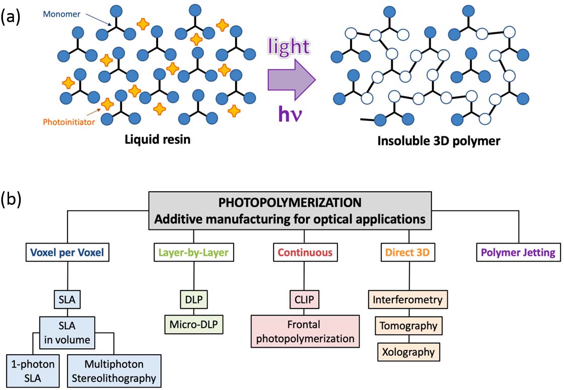
    Fig. 1. (a) Simplified schematic of the photopolymerization process involving the main components (photoinitiator and monomer). (b) The main photopolymerization-based additive manufacturing techniques described in this review.
    (a) Schematic representation of the radical photopolymerization process involving a photoinitiator (PI) absorbing a photon of energy hν to reach an excited state (PI*). From this excited state, radical species are generated, which initiate the radical polymerization of monomers (M). (b) The examples of acrylate monomers with low and high refractive index monomers. (c) The example of photoinitiators and radical species created by UV photolysis of these photoinitiators. (d) The molecular processes of inhibition of radical polymerization by oxygen.
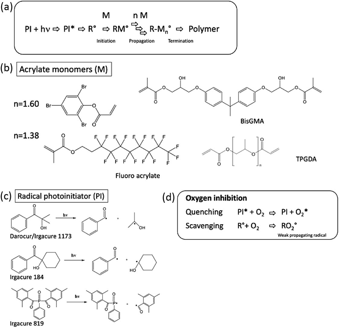
    Fig. 2. (a) Schematic representation of the radical photopolymerization process involving a photoinitiator (PI) absorbing a photon of energy hν to reach an excited state (PI*). From this excited state, radical species are generated, which initiate the radical polymerization of monomers (M). (b) The examples of acrylate monomers with low and high refractive index monomers. (c) The example of photoinitiators and radical species created by UV photolysis of these photoinitiators. (d) The molecular processes of inhibition of radical polymerization by oxygen.
    (a) Examples of acrylate (green) and thiol-ene (red-blue) monomers used in volumetric additive manufacturing, and the schematic structure of the prepared polymers. (b) An example of the 3D objects (scale bar 5 mm). (c) The illustration of the modularity of mechanical properties obtained using the thiol-ene systems [36].
    Fig. 3. (a) Examples of acrylate (green) and thiol-ene (red-blue) monomers used in volumetric additive manufacturing, and the schematic structure of the prepared polymers. (b) An example of the 3D objects (scale bar 5 mm). (c) The illustration of the modularity of mechanical properties obtained using the thiol-ene systems [36].
    (a) Schematic representation of the cationic photopolymerization process. (b) The photolysis mechanism of an iodonium salt. (c) The examples of epoxy monomers used in cationic photopolymerization.
    Fig. 4. (a) Schematic representation of the cationic photopolymerization process. (b) The photolysis mechanism of an iodonium salt. (c) The examples of epoxy monomers used in cationic photopolymerization.
    Schematic view of the benefit of using a thermal post-cure versus UV post-cure. Thermal post-curing results in better homogeneity in the core of the polymer object. (a)–(f) are SEM images with different magnification of an object prepared by SLA with (a), (c), (e) UV post-cure and (b), (d), (f) thermal post-cure. The difference in structure is clearly visible by comparing (e) and (f). Bulk and surface homogeneity are critical parameters for optical applications [47].
    Fig. 5. Schematic view of the benefit of using a thermal post-cure versus UV post-cure. Thermal post-curing results in better homogeneity in the core of the polymer object. (a)–(f) are SEM images with different magnification of an object prepared by SLA with (a), (c), (e) UV post-cure and (b), (d), (f) thermal post-cure. The difference in structure is clearly visible by comparing (e) and (f). Bulk and surface homogeneity are critical parameters for optical applications [47].
    (a) Hybrid material approach based on organic/inorganic hybrid precursors in the context of 3D manufacturing by photopolymerization. The three precursors used react in solution by hydrolysis-condensation reactions (sol-gel chemistry) to form an inorganic network, which is cross-linked by UV irradiation. Examples of transparent parts are given (scale bar, 1 cm) [50]. (b) Nanocomposite approach by introducing silica nanoparticles in a light-curing matrix to fabricate 3D nanocomposite objects and subsequently sintering to mineralize the material. The examples of transparent silica parts that were made by this process are given (scale bar, 5 mm) [51].
    Fig. 6. (a) Hybrid material approach based on organic/inorganic hybrid precursors in the context of 3D manufacturing by photopolymerization. The three precursors used react in solution by hydrolysis-condensation reactions (sol-gel chemistry) to form an inorganic network, which is cross-linked by UV irradiation. Examples of transparent parts are given (scale bar, 1 cm) [50]. (b) Nanocomposite approach by introducing silica nanoparticles in a light-curing matrix to fabricate 3D nanocomposite objects and subsequently sintering to mineralize the material. The examples of transparent silica parts that were made by this process are given (scale bar, 5 mm) [51].
    (a) Principle of the SLA [70]. (b) An example of the lenses manufactured by SLA, after production, and surface treatments by dipping in resins and polymerization (left, finished product) [71]. (c) The typical example of a surface defect [72]. (d) The examples of objects made with micro-SLA [73].
    Fig. 7. (a) Principle of the SLA [70]. (b) An example of the lenses manufactured by SLA, after production, and surface treatments by dipping in resins and polymerization (left, finished product) [71]. (c) The typical example of a surface defect [72]. (d) The examples of objects made with micro-SLA [73].
    (a) Experimental setup for low one-photon absorption (LOPA) photolithography. (b) Absorption spectrum of the resin (SU8) showing the very low absorbance of the resin at the wavelength used (532 nm). (c) and (d) Examples of structures prepared by LOPA [78,79].
    Fig. 8. (a) Experimental setup for low one-photon absorption (LOPA) photolithography. (b) Absorption spectrum of the resin (SU8) showing the very low absorbance of the resin at the wavelength used (532 nm). (c) and (d) Examples of structures prepared by LOPA [78,79].
    Examples of optical microelements fabricated by biphotonic stereolithography [87,88].
    Fig. 9. Examples of optical microelements fabricated by biphotonic stereolithography [87,88].
    (a) DLP technology with grayscale writing. (b) An example of a lens made by DLP using the post-polymerized meniscus strategy and grayscale writing. (c) The comparison between the classical DLP approach (top) and post-polymerization and grayscale approach [112].
    Fig. 10. (a) DLP technology with grayscale writing. (b) An example of a lens made by DLP using the post-polymerized meniscus strategy and grayscale writing. (c) The comparison between the classical DLP approach (top) and post-polymerization and grayscale approach [112].
    (a) Schematic diagram of the CLIP technology [114]. (b) Schematic diagram of the CLIP technology with the photoinhibitor [116]. (c) The illustration of the influence of the choice of slicing on the roughness of objects manufactured by CLIP [115]. (d) The examples of lenses manufactured by micro-CLIP. The roughness suppression on the right example is obtained by depositing a resin layer in post-processing [117].
    Fig. 11. (a) Schematic diagram of the CLIP technology [114]. (b) Schematic diagram of the CLIP technology with the photoinhibitor [116]. (c) The illustration of the influence of the choice of slicing on the roughness of objects manufactured by CLIP [115]. (d) The examples of lenses manufactured by micro-CLIP. The roughness suppression on the right example is obtained by depositing a resin layer in post-processing [117].
    (a) Schematic diagram of the FPP approach [118]. (b) The example of 3D objects manufactured by FPP based on different monomer chemistries [119]. (c) The examples of micro-lenses manufactured by FPP at the end of an optical fiber [120].
    Fig. 12. (a) Schematic diagram of the FPP approach [118]. (b) The example of 3D objects manufactured by FPP based on different monomer chemistries [119]. (c) The examples of micro-lenses manufactured by FPP at the end of an optical fiber [120].
    (a) Schematic of the polymer jetting technique [129]. (b) The example of a lens (center) made from the model (left) and the characterization of the surface (right) [129]. (c) The characterization of the surface roughness of the objects [131].
    Fig. 13. (a) Schematic of the polymer jetting technique [129]. (b) The example of a lens (center) made from the model (left) and the characterization of the surface (right) [129]. (c) The characterization of the surface roughness of the objects [131].
    (a) Scheme of the experimental set-up for the volumetric AM in one step and examples of realizations. (b) The comparison of the performance of this technique with the main AM techniques [136].
    Fig. 14. (a) Scheme of the experimental set-up for the volumetric AM in one step and examples of realizations. (b) The comparison of the performance of this technique with the main AM techniques [136].
    (a) Schematic of the axial volume lithography technique, (b) schematic of the device, (c) photographs of the sample being fabricated, and (d) examples of objects fabricated with this technique in different materials and sizes [137].
    Fig. 15. (a) Schematic of the axial volume lithography technique, (b) schematic of the device, (c) photographs of the sample being fabricated, and (d) examples of objects fabricated with this technique in different materials and sizes [137].
    (a) Schematic of the xolography technique and specific photocommutable photoinitiator synthesized at the base of this approach. The spectrum of the photoinitiator in its initial form is in black, and after irradiation in the UV (λ1=375 nm), it switches to a shape that has an absorption band in the visible (blue spectrum). (b) Examples of objects made with the xolography technique [141].
    Fig. 16. (a) Schematic of the xolography technique and specific photocommutable photoinitiator synthesized at the base of this approach. The spectrum of the photoinitiator in its initial form is in black, and after irradiation in the UV (λ1=375  nm), it switches to a shape that has an absorption band in the visible (blue spectrum). (b) Examples of objects made with the xolography technique [141].
    Emma Geisler, Maxime Lecompère, Olivier Soppera. 3D printing of optical materials by processes based on photopolymerization: materials, technologies, and recent advances[J]. Photonics Research, 2022, 10(6): 1344
    Download Citation