• Opto-Electronic Advances
  • Vol. 6, Issue 4, 220034 (2023)
Jiajie Pei1、2, Xue Liu3, Andrés Granados del Águila3, Di Bao3, Sheng Liu3, Mohamed-Raouf Amara3, Weijie Zhao3, Feng Zhang1, Congya You4, Yongzhe Zhang4, Kenji Watanabe5, Takashi Taniguchi5, Han Zhang1、*, and Qihua Xiong6、**
Author Affiliations
  • 1Collaborative Innovation Center for Optoelectronic Science and Technology, International Collaborative Laboratory of 2D Materials for Optoelectronic Science and Technology of Ministry of Education and Guangdong Province, College of Optoelectronic Engineering, Shenzhen University, Shenzhen 518060, China
  • 2College of Materials Science and Engineering, Fuzhou University, Fuzhou 350108, China
  • 3Division of Physics and Applied Physics, School of Physical and Mathematical Sciences, Nanyang Technological University, Singapore 637371, Singapore
  • 4College of Materials Science and Engineering, Beijing University of Technology, Beijing 100124, China
  • 5Research Center for Functional Materials, International Center for Materials Nanoarchitectonics, National Institute for Materials Science, Tsukuba, Ibaraki 305-0044, Japan
  • 6State Key Laboratory of Low Dimensional Quantum Physics and Department of Physics, Tsinghua University, Beijing 100084, China
  • show less
    DOI: 10.29026/oea.2023.220034 Cite this Article
    Jiajie Pei, Xue Liu, Andrés Granados del Águila, Di Bao, Sheng Liu, Mohamed-Raouf Amara, Weijie Zhao, Feng Zhang, Congya You, Yongzhe Zhang, Kenji Watanabe, Takashi Taniguchi, Han Zhang, Qihua Xiong. Switching of K-Q intervalley trions fine structure and their dynamics in n-doped monolayer WS2[J]. Opto-Electronic Advances, 2023, 6(4): 220034 Copy Citation Text show less
    Schematic diagram and device characterization. (a) Schematic drawing of the spin configurations for monolayer WS2 in the conduction band and valence band at K and K’ point of the first Brillouin zone. The bands with two different spin configurations are schematically drawn using two different colors (blue and red), annotated with arrows representing different spins. The symbols “e” and “h” represent electrons and holes, respectively. Scattering pathways of electrons are denoted by the orange arrows. The green wavy arrow represents the excitation photons. (b) The possible valley exciton and trions emissions from KV valley in the momentum space. Upon linear optical excitation, the landscape of excitons and trions with opposite spin configurations degenerates. Here, we display the valley excitons and trions for only one spin configuration. Fermi level changes are represented by orange and green dashed lines. The Coulomb interactions of exciton and trions are denoted by the filled areas with red, orange, and green colors. (c) Optical micrograph of the h-BN/1L-WS2/h-BN sandwiched sample. The scale bar is 5 μm. (d) Schematic plot of the heterostructure device. (e) The drain-source current as a function of back-gate voltage for various source-drain biases. With this transition curve, it is found the WS2 monolayer is an n-type semiconductor. Note that the gate-dependent PL measurement in the main text is measured at zero source-drain bias.
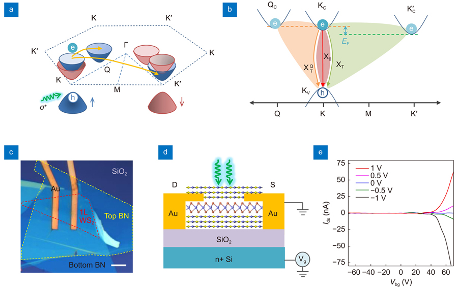
    Fig. 1. Schematic diagram and device characterization. (a) Schematic drawing of the spin configurations for monolayer WS2 in the conduction band and valence band at K and K’ point of the first Brillouin zone. The bands with two different spin configurations are schematically drawn using two different colors (blue and red), annotated with arrows representing different spins. The symbols “e” and “h” represent electrons and holes, respectively. Scattering pathways of electrons are denoted by the orange arrows. The green wavy arrow represents the excitation photons. (b) The possible valley exciton and trions emissions from KV valley in the momentum space. Upon linear optical excitation, the landscape of excitons and trions with opposite spin configurations degenerates. Here, we display the valley excitons and trions for only one spin configuration. Fermi level changes are represented by orange and green dashed lines. The Coulomb interactions of exciton and trions are denoted by the filled areas with red, orange, and green colors. (c) Optical micrograph of the h-BN/1L-WS2/h-BN sandwiched sample. The scale bar is 5 μm. (d) Schematic plot of the heterostructure device. (e) The drain-source current as a function of back-gate voltage for various source-drain biases. With this transition curve, it is found the WS2 monolayer is an n-type semiconductor. Note that the gate-dependent PL measurement in the main text is measured at zero source-drain bias.
    Electrical tuning of the PL spectra of excitonic species. (a) A typical PL spectrum of the monolayer WS2 at T=10 K excited by 2.33 eV laser. The label X0 and XT represent bright exciton and trion, respectively. The labelsXTQrepresents Q-valley charged state, and the rest three peaks are labeled as Ls representing localized states. (b) Color plot of the measured PL spectra for monolayer WS2 as a function of back-gate voltage at 25 μW excitation power. The black dashed lines are a guide to the eye showing the positions of the emission peaks. The red dashed arrow illustrates the transition trend for XX– peak intensity under doping, which should be opposite to theXTQfeature. (c) Integrated PL intensities of the X0 (black circle), XT (blue circle), andXTQ(red triangle) as a function of back-gate voltage. The solid lines are fitting results with the equations in Supplementary information Section 2.
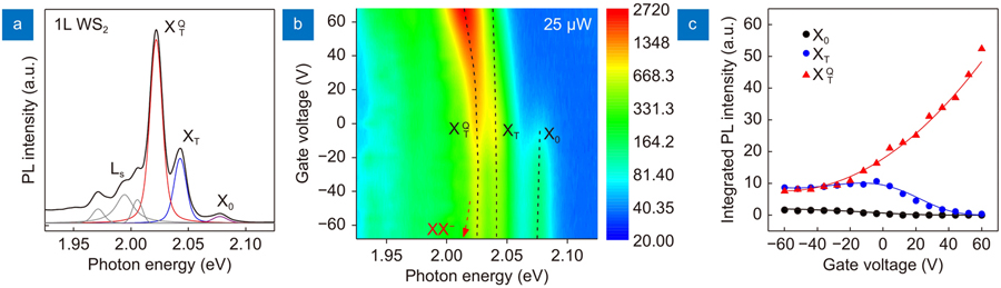
    Fig. 2. Electrical tuning of the PL spectra of excitonic species. (a) A typical PL spectrum of the monolayer WS2 at T=10 K excited by 2.33 eV laser. The label X0 and XT represent bright exciton and trion, respectively. The labels XTQ represents Q-valley charged state, and the rest three peaks are labeled as Ls representing localized states. (b) Color plot of the measured PL spectra for monolayer WS2 as a function of back-gate voltage at 25 μW excitation power. The black dashed lines are a guide to the eye showing the positions of the emission peaks. The red dashed arrow illustrates the transition trend for XX peak intensity under doping, which should be opposite to the XTQ feature. (c) Integrated PL intensities of the X0 (black circle), XT (blue circle), and XTQ (red triangle) as a function of back-gate voltage. The solid lines are fitting results with the equations in Supplementary information Section 2.
    Influence of electrical doping on the carrier dynamics of excitonic species. (a, b) Normalized PL spectra at per μW excitation power for monolayer WS2 as a function of excitation power at –60 V and 60 V back gate voltages. The dashed lines are guided to the eye showing the peak positions of X0 andXTQ. (c) Log-log plot of the integrated PL intensity forXTQ as a function of excitation power and gate voltage from –60 V to 60 V. The solid lines are power-law fittings with IPL=Pα. The dashed line is guided to the eye showing the power-low slope of α=1. Insert illustrates the electron concentration in the direct and indirect valley at low and high doping and pumping. (d) Measured time-resolved PL traces (dots) for the XT andXTQ at a temperature of 10 K with pulsed laser excitation at a photon energy of 3.1 eV and power of 0.5 μW. The dashed line IRF is the instrument response function. The solid lines are double exponential fitting using the equation I = Aexp(−t/τ1) + Bexp(−t/τ2) + C based on the convolution with respect to the instrument response. The fast decay lifetime τ1 for the XT andXTQ were extracted to be 20.9±2 ps and 38.5±2 ps, respectively. The slow decay lifetime τ2 for the XT andXTQ were extracted to be 249±8 ps and 316±5 ps, respectively. (e) Measured time-resolved PL traces (dots) for theXTQ at different back-gate voltages (from –60 V to 60 V). The solid lines are corresponding double exponential fitting curves. (f) The statistical values of the fast decay lifetime τ1 and slow decay lifetime τ2 for the fitting results of XT andXTQ at different back-gate voltages.
    Fig. 3. Influence of electrical doping on the carrier dynamics of excitonic species. (a, b) Normalized PL spectra at per μW excitation power for monolayer WS2 as a function of excitation power at –60 V and 60 V back gate voltages. The dashed lines are guided to the eye showing the peak positions of X0 andXTQ. (c) Log-log plot of the integrated PL intensity forXTQ as a function of excitation power and gate voltage from –60 V to 60 V. The solid lines are power-law fittings with IPL=Pα. The dashed line is guided to the eye showing the power-low slope of α=1. Insert illustrates the electron concentration in the direct and indirect valley at low and high doping and pumping. (d) Measured time-resolved PL traces (dots) for the XT andXTQ at a temperature of 10 K with pulsed laser excitation at a photon energy of 3.1 eV and power of 0.5 μW. The dashed line IRF is the instrument response function. The solid lines are double exponential fitting using the equation I = Aexp(−t1) + Bexp(−t2) + C based on the convolution with respect to the instrument response. The fast decay lifetime τ1 for the XT andXTQ were extracted to be 20.9±2 ps and 38.5±2 ps, respectively. The slow decay lifetime τ2 for the XT andXTQ were extracted to be 249±8 ps and 316±5 ps, respectively. (e) Measured time-resolved PL traces (dots) for theXTQ at different back-gate voltages (from –60 V to 60 V). The solid lines are corresponding double exponential fitting curves. (f) The statistical values of the fast decay lifetime τ1 and slow decay lifetime τ2 for the fitting results of XT andXTQ at different back-gate voltages.
    Temperature-dependent PL spectra of the monolayer WS2. (a) PL spectra at different temperatures from 295 K to 10 K. The spectra are vertically shifted for clarity. The dashed lines are a guide to the eye showing the peak positions of X0, XT andXTQ. (b) Peak energy of X0, XT andXTQ emissions in dependence of temperature. The solid lines are fitting curves with a standard semiconductor bandgap dependence: Eg(T) = Eg(0)−Sℏω[coth(ℏω/2kBT)−1], where Eg(0) is the ground state transition energy at 0 K, S is a dimensionless coupling constant and ħω is an average phonon energy. The fitting parameters for X0 are: Eg(0)=2.08 eV, S =1.807, ħω=11.91 meV; the fitting parameters for XT are: Eg(0)= 2.043 eV, S = 2.038, ħω= 14.69 meV; the fitting parameters forXTQ are: Eg(0)= 2.022 eV, S = 1.373, ħω= 13.6 meV. (c) Integrated PL intensity of X0, XT, andXTQ emissions in dependence of temperature. The solid lines are fitting curves with the equations in Supplementary information Section 1. The violet dashed line is the sum of the red and blue solid curves. (d) Schematic drawing of the thermalization induced shrinking and expansion of lattice and related bandgap renormalization. (e) The Q-K valley energy difference at each temperature that extracted from the fit of the experimental results in c based on the equations in Supplementary information Section 1. The temperature-dependent ΔEQK is about twice the energy offset value of the X0 peak, which implies that the offset between the K-Q valleys is in the opposite direction.
    Fig. 4. Temperature-dependent PL spectra of the monolayer WS2. (a) PL spectra at different temperatures from 295 K to 10 K. The spectra are vertically shifted for clarity. The dashed lines are a guide to the eye showing the peak positions of X0, XT andXTQ. (b) Peak energy of X0, XT andXTQ emissions in dependence of temperature. The solid lines are fitting curves with a standard semiconductor bandgap dependence: Eg(T) = Eg(0)−Sω[coth(ω/2kBT)−1], where Eg(0) is the ground state transition energy at 0 K, S is a dimensionless coupling constant and ħω is an average phonon energy. The fitting parameters for X0 are: Eg(0)=2.08 eV, S =1.807, ħω=11.91 meV; the fitting parameters for XT are: Eg(0)= 2.043 eV, S = 2.038, ħω= 14.69 meV; the fitting parameters forXTQ are: Eg(0)= 2.022 eV, S = 1.373, ħω= 13.6 meV. (c) Integrated PL intensity of X0, XT, andXTQ emissions in dependence of temperature. The solid lines are fitting curves with the equations in Supplementary information Section 1. The violet dashed line is the sum of the red and blue solid curves. (d) Schematic drawing of the thermalization induced shrinking and expansion of lattice and related bandgap renormalization. (e) The Q-K valley energy difference at each temperature that extracted from the fit of the experimental results in c based on the equations in Supplementary information Section 1. The temperature-dependent ΔEQK is about twice the energy offset value of the X0 peak, which implies that the offset between the K-Q valleys is in the opposite direction.
    Jiajie Pei, Xue Liu, Andrés Granados del Águila, Di Bao, Sheng Liu, Mohamed-Raouf Amara, Weijie Zhao, Feng Zhang, Congya You, Yongzhe Zhang, Kenji Watanabe, Takashi Taniguchi, Han Zhang, Qihua Xiong. Switching of K-Q intervalley trions fine structure and their dynamics in n-doped monolayer WS2[J]. Opto-Electronic Advances, 2023, 6(4): 220034
    Download Citation