Abstract
Monolayer group VI transition metal dichalcogenides (TMDs) have recently emerged as promising candidates for photonic and opto-valleytronic applications. The optoelectronic properties of these atomically-thin semiconducting crystals are strongly governed by the tightly bound electron-hole pairs such as excitons and trions (charged excitons). The anomalous spin and valley configurations at the conduction band edges in monolayer WS2 give rise to even more fascinating valley many-body complexes. Here we find that the indirect Q valley in the first Brillouin zone of monolayer WS2plays a critical role in the formation of a new excitonic state, which has not been well studied. By employing a high-quality h-BN encapsulated WS2 field-effect transistor, we are able to switch the electron concentration within K-Q valleys at conduction band edges. Consequently, a distinct emission feature could be excited at the high electron doping region. Such feature has a competing population with the K valley trion, and experiences nonlinear power-law response and lifetime dynamics under doping. Our findings open up a new avenue for the study of valley many-body physics and quantum optics in semiconducting 2D materials, as well as provide a promising way of valley manipulation for next-generation entangled photonic devices.Introduction
Transition metal dichalcogenides (TMDs) have attracted great attention as potential candidates for novel optoelectronic applications1, 2 in recent years, due to their unique excitonic properties and strong many-body effects3. The tightly bound electron-hole quasiparticles (exciton, trion, biexciton, etc.) that originated from the excitonic effect are extremely crucial for the optoelectronic properties of TMDs as well as their devices4-9. The coupling of valleys to excitonic states gives rise to the so-called valley many-body complexes10-13, which provide the possibility of manipulating the valley index via optical probes. Their unique properties provide an attractive platform for research in fundamental physics, quantum optics, valleytronics, etc14-24.
For molybdenum compounds (MoS2, MoSe2), normally two main excitonic species are observed in the photoluminescence (PL) spectra, namely exciton and trion7, 8, 25, 26, owning to their aligned spin in the conduction band minimum (CB) and the valance band maximum (VB). In contrast, recent studies have proved that the tungsten compounds (WS2, WSe2) have an opposite spin configuration in the conduction band minimum and the valence band maximum27-29, which significantly affects their excitonic emissions, underpinning even more fascinating valley excitonic states in those compounds. For instance, the brightening of spin-dark exciton9, 30, 31, the observation of biexciton32-34, or even higher-order many-body complex6, 35, 36 have been reported. Normally the direct K and K’ valleys were considered during the interpretation of such excitonic states. The indirect Q valley (sometimes also referred to as Λ or Σ), which possesses the same spin and very close energy level to the K valley in the first Brillouin zone of monolayer WS237-39, has received less attention. Such valley was recently found to significantly influence the excited-state distribution under the above-gap excitation40-42. Whereas the impact of Q valley on the formation of valley many-body complexes has not been well studied so far. To unravel the exact nature of the emissions, it is crucial to probe the transition processes of the many-body species while modulating the carrier densities within different valleys at conduction band edges.
Here we probed the indirect Q-valley charged states by tuning the Fermi energy with a high-quality h-BN encapsulated WS2 field-effect transistor. A distinct emission feature manifests itself as ~20 meV lower in energy and competing population with the conventional trion of monolayer WS2 was stimulated when the sample is exposed to high excitation power or under high electron doping. We found that the actual doping level of the sample has a significant impact on the power-law response of this emission feature. And the carrier lifetime of such an excitonic state probed by the time-resolved photoluminescence (TRPL) measurement also shows a strong gate dependence. The nonlinear power and gate response were due to the changing Fermi level-induced variation of the dark exciton population. Our study reveals the critical role of the indirect Q valley in the formation of valley many-body complexes, as well as provides an efficient way of manipulating such complexes in transition metal dichalcogenides for future opto-valleytronic applications.
Results
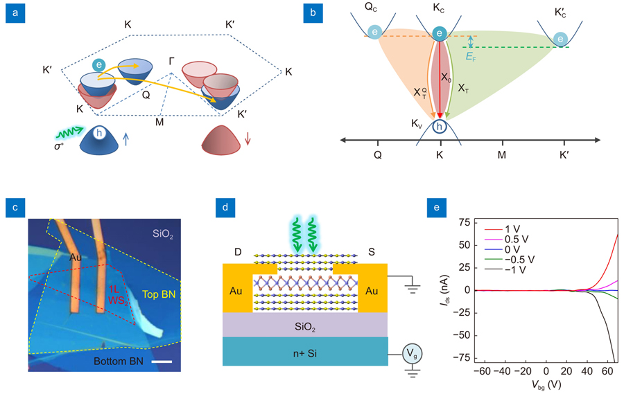
Upon photoexcitation at the WS2 monolayer, the electrons and holes are generated and then bound together at energy degenerate valleys of the first Brillouin zone (Fig. 1(a)), giving rise to various types of valley excitons and trions10-13. Previous studies found that the conduction band of monolayer WS2 has ~35 meV of spin splitting at the K valley of the first Brillouin zone, while the spin of conduction band minimum is opposite to the valance band maximum27, 29, 37. The spin configurations of the conduction band and valence band are illustrated in Fig. 1(a) with arrows and different colors. Such spin-opposite valleys at K/K' points of the conduction band have been studied extensively. Recent calculations show that the Coulomb interaction of electron-hole pairs in the intermediate Q valley is rather strong (70~100 meV larger than the K valley exciton) in WSe2/WS2, due to the much larger effective mass of the Q valley compared to the K valley27, 29. This has been proved recently in experiments with time-resolved XUV micro-angle resolved photoemission spectroscopy for WSe240 and WS241, where the momentum-indirect Q valley excitons were found to be rather significant.

Figure 1.Schematic diagram and device characterization. (a) Schematic drawing of the spin configurations for monolayer WS2 in the conduction band and valence band at K and K’ point of the first Brillouin zone. The bands with two different spin configurations are schematically drawn using two different colors (blue and red), annotated with arrows representing different spins. The symbols “e” and “h” represent electrons and holes, respectively. Scattering pathways of electrons are denoted by the orange arrows. The green wavy arrow represents the excitation photons. (b) The possible valley exciton and trions emissions from KV valley in the momentum space. Upon linear optical excitation, the landscape of excitons and trions with opposite spin configurations degenerates. Here, we display the valley excitons and trions for only one spin configuration. Fermi level changes are represented by orange and green dashed lines. The Coulomb interactions of exciton and trions are denoted by the filled areas with red, orange, and green colors. (c) Optical micrograph of the h-BN/1L-WS2/h-BN sandwiched sample. The scale bar is 5 μm. (d) Schematic plot of the heterostructure device. (e) The drain-source current as a function of back-gate voltage for various source-drain biases. With this transition curve, it is found the WS2 monolayer is an n-type semiconductor. Note that the gate-dependent PL measurement in the main text is measured at zero source-drain bias.
The photoexcited electrons at K valley could be scattered either to the K' or Q valley via phonon (Fig. 1(a)) to form the so-called dark excitons27, 41, 42. Strong exciton binding energies of such excitons make them energetically more favorable than the K valley bright exciton in WS2. However, they are normally not observable in the PL spectra due to the nonzero center-of-mass momentum. When the sample is electrically n doped, both the K' or Q valleys can be filled with electrons that interact with the K valley exciton directly to form the so-called intervalley trions, as illustrated in Fig. 1(b). These configurations give rise to two types of intervalley trions XT and in WS2. The former type has been classified as a trion fine structure previously11, 13, while the latter one has not been reported before.
We conducted optical spectroscopy measurement of a monolayer WS2 sample, configured as a typical field-effect transistor, to unravel the emission species upon the back-gate potential modulation. As shown in Fig. 1(c) and 1(d), the monolayer WS2 sample is encapsulated by two pieces of few-layer high-quality h-BN to minimize the influence of surface defect states on the PL spectra6, 30. The WS2 sample is grounded and the back gate voltage is applied to the degenerately doped n+ Si substrate with a 300 nm thickness SiO2 as the dielectric layer. The as-prepared FET displays an n-channel depletion mode behavior with a turn-on voltage of ~45 V (Fig. 1(e)).
The PL spectrum of the sample measured at zero gate voltage at 10 K is shown in Fig. 2(a). Six PL emission features are clearly observed: the peak with the highest energy ~2.075 eV arising from the exciton (X0); the associated negatively charged exciton (XT) at ~37 meV below X0; three lower-energy peaks labeled as Ls which are normally attributed to localized states30, 34 or related to the valley phonon replicas of dark trions43. The fine structure of trion XT could not be resolved in our measurements, possibly because of peak broadening due to electron doping or insufficiently low sample temperature. The most prominent peak () located at ~2.025 eV is the focus of our current study. Fig. 2(b) shows the color contour plot of the PL spectra at different doping densities (corresponding to back-gate voltages from –60 V to 60 V). As the doping density of electrons is increased, the intensity of the X0 peak decreases gradually, while the intensity of XT peak and peak increase slowly from –60 V to 0 V. When the back gate voltage increases from 0 V to 60 V, the X0 peak disappears and the intensity of XT peak drops rapidly. On the contrary, the intensity of peak grows dramatically until it becomes dominant in the spectrum at 60 V as a result of increased Fermi level. On the other hand, the increase of Fermi level will enlarge the magnitude of Stokes shift8, resulting in a peak red-shift of the trion XT and XTQ with increasing electron doping (Fig. 2(b)). Figure 2(c) shows the integrated PL intensities of such emission features, extracted from detailed fitting results of all peaks as shown inFig. S1. It is interesting to found the intensities of XT and appear to be a competitive relationship that can be switched by the gate (Fig. 2(c)), which follows the Boltzmann distribution (will be calculated later in Supplementary information Section 2).
Figure 2.Electrical tuning of the PL spectra of excitonic species. (a) A typical PL spectrum of the monolayer WS2 at T=10 K excited by 2.33 eV laser. The label X0 and XT represent bright exciton and trion, respectively. The labels
represents Q-valley charged state, and the rest three peaks are labeled as Ls representing localized states. (b) Color plot of the measured PL spectra for monolayer WS2 as a function of back-gate voltage at 25 μW excitation power. The black dashed lines are a guide to the eye showing the positions of the emission peaks. The red dashed arrow illustrates the transition trend for XX– peak intensity under doping, which should be opposite to the
feature. (c) Integrated PL intensities of the X0 (black circle), XT (blue circle), and
(red triangle) as a function of back-gate voltage. The solid lines are fitting results with the equations in Supplementary information Section 2.
The power-law analysis was normally used to further characterize the nature of excitonic complexes3. However, we found that the power-law trend of varies with the actual doping of the sample (Fig. 3(a, b), which could be due to the variation of exciton/trion population induced by Fermi level changing. The corresponding integrated PL intensity for peak as a function of excitation power is shown in Fig. 3(c). When the sample is at –60 V back gate tuning, the power-law slope of such a peak is α~1.42. Meanwhile, the increase of exciton X0 as a function of excitation power becomes sublinear with a power-law slope of α~0.84, while the power-law slope for the trion XT is α~1.16 (Fig. S2). A transition from excitons to trions occurs as the excitation power increases. In contrast, when the sample is heavily n-doped (at 60 V back gate tuning), the power-law slope of becomes α~0.95 (Fig. 3(c)), which means that the PL intensity of such feature is increasing near linear with the excitation. The power-law slope of the could be tuned continuously from 1.42 to 0.95 by swapping the back gate voltage from –60 V to 60 V (Fig. 3(c)). Due to the variation of the power-law slope with sample doping, it is important to note that the feature is unlikely to be a biexciton emission as previously reported32, 44. Actually, it has been well accepted recently that the binding energy of biexciton (~24 meV) is smaller than that of the trion36, 45.
Figure 3.Influence of electrical doping on the carrier dynamics of excitonic species. (a, b) Normalized PL spectra at per μW excitation power for monolayer WS2 as a function of excitation power at –60 V and 60 V back gate voltages. The dashed lines are guided to the eye showing the peak positions of X0 and. (c) Log-log plot of the integrated PL intensity for as a function of excitation power and gate voltage from –60 V to 60 V. The solid lines are power-law fittings with IPL=Pα. The dashed line is guided to the eye showing the power-low slope of α=1. Insert illustrates the electron concentration in the direct and indirect valley at low and high doping and pumping. (d) Measured time-resolved PL traces (dots) for the XT and at a temperature of 10 K with pulsed laser excitation at a photon energy of 3.1 eV and power of 0.5 μW. The dashed line IRF is the instrument response function. The solid lines are double exponential fitting using the equation I = Aexp(−t/τ1) + Bexp(−t/τ2) + C based on the convolution with respect to the instrument response. The fast decay lifetime τ1 for the XT and were extracted to be 20.9±2 ps and 38.5±2 ps, respectively. The slow decay lifetime τ2 for the XT and were extracted to be 249±8 ps and 316±5 ps, respectively. (e) Measured time-resolved PL traces (dots) for the at different back-gate voltages (from –60 V to 60 V). The solid lines are corresponding double exponential fitting curves. (f) The statistical values of the fast decay lifetime τ1 and slow decay lifetime τ2 for the fitting results of XT and at different back-gate voltages.
The gate-dependent power-law responses can be explained as follows. For the –60 V back gate tuning, the Fermi level is below the lower indirect valley. Upon low-power excitation, most of the electrons are scattered into the lower-lying valley forming the dark excitons. Only a small amount of the photoexcited electrons participates in the photoluminescence process from the direct valley, as illustrated in the schematic diagram inserted at the bottom of Fig. 3(c). As the excitation power increases, the electron density in the indirect valley will continue to increase until it finally reaches saturation. Most of the electrons still remain in the direct valley, as illustrated in the right upper panel of Fig. 3(c). Thus, the total PL emission experienced a super-linear increase from low power to high power. For the 60 V situation, the indirect valley has already been filled with electrons by doping (left upper panel in Fig. 3(c)). At each power, the photoexcited electrons will recombine through the direct valley efficiently rather than scattering to other valleys. That explains why the power-law slope of the PL emission was close to 1 under 60 V back gate voltage.
Time-resolved photoluminescence (TRPL) measurement (Methods) was used to further probe the carrier dynamics of such excitonic species. Figure 3(d) shows the normalized TRPL spectra for the XT and emission features. Note that the fast X0 process is not discussed here since it approaches our instrument limit. The TRPL spectra experience a similar fast rise at the beginning, but the following decay processes differ significantly. For the trion XT, the decay process contains two distinct time scales, namely a fast decay (τ1) with ~85% of the weight and a slow decay (τ2) with ~15% of the weight. By a double exponential fitting, the values of τ1 and τ2 for the XT are extracted to be (20.9±2) ps and (249±8) ps, respectively. The fast decay τ1 of tens of picoseconds has been attributed to the nonradiative decay lifetime caused by the carrier-carrier scattering or carrier-phonon scattering, while the slow decay τ2 of hundreds of picoseconds is the radiative decay lifetime that is related to the interband electron-hole recombination46, 47. In contrast, the values of τ1 (~38.5±2 ps) and τ2 (~316±5 ps) for the emission are much longer, and the weight of radiative decay (~60%) is more prominent (Fig. 3(d)). More interestingly, the decay process of the emission shows a strong gate dependence (Fig. 3(e–f)), whereas the trion XT has negligible change as the gate changes (Fig. 3(f) andFig. S3).
On the other hand, we observed similar results by changing the excitation powers, as shown in Fig. S4. The radiative lifetime (τ2) of XT does not show a noticeable change as a function of laser power. However, the radiative lifetime (τ2) of decreases from 530 ps to 328 ps, when we increase the laser power from 0.2 μW to 4 μW. These results indicate that the increase of laser power experiences a similar process of carrier dynamics to the electron doping in monolayer WS2. The nonlinear carrier dynamics of the feature implies the transition relationship between these two types of trions. At each Fermi level, the electrons scattering to the K'C valley are always efficient due to their lower energy. Thus, the radiative lifetime (τ2) of XT trion is always short and has an inconspicuous response to the doping (Fig. 3(f)). While in terms of the trion formation, it is suppressed at low Fermi levels but becomes more favorable when the Fermi level reaches the QC valley as a result of the stronger binding strength of QC-KV electron-hole pairs27, 29. Thus, the radiative lifetime (τ2) of trion experiences a dramatic decrease until it reaches the same timescale (250 ps) as the XT (Fig. 3(f)) under doping.
At last, we show that the switching between such two types of intervalley trions could be observed as well due to the thermalization induced K-Q valley energy variation (Fig. 4(a)). As the temperature decreases from 295 K, the intensity of X0 peak decreases gradually, while the intensity of XT peak increases first and then followed by a fast decay after 110 K. Meanwhile, the peak starts to emerge at around 110 K. For quantitative analysis, the peak energies and integrated PL intensities of such emission features are collected in Fig. 4(b, c), extracted from detailed fitting results as shown inFig. S5. All the three peaks experience a blue shift when the temperature decreases, and the peak energies can be fit well (Fig. 4(b)) using a standard semiconductor bandgap dependence equation7. The integrated PL intensities of such emission features fit with the model provided in Supplementary information Section 1. Noticed that the total emission of XT and follows a monotonic increasing trend (Fig. 4(c), violet curve) as a function of temperature. Thus, in the calculation, we first estimated the populations of the neutral (X) and charged states (X–) using the mass action model7. Then, the populations of neutral and charged states were further split into two substructures, as a result of the energy splitting of them. The concentration of energy-split substructures at each temperature could be estimated with the Boltzmann distribution28 (Supplementary information Section 1). Here, a calibration of the Q-K valley energy difference (ΔEQK) at each temperature is necessary. According to the density functional theory calculation39, the temperature variation induced strain can result in a band renormalization that changes the value of ΔEQK, i.e., the bandgap expands at the K valley and contracts at the Q valley when the sample is subjected to compressive strain, as illustrated in Fig. 4(d). The calculated result matches well with the experimental data (Fig. 4(c) &Fig. S6) by adding this term into the Boltzmann distribution equation (Supplementary information Section 1). The Q-K valley energy difference as a function of temperature was fit to be as ΔEQK = 15+0.24(kBT)2, and the temperature-dependent curve is shown in Fig. 4(e). Since the peak energy of exciton X0 is blue-shifted (Fig. 4(b)) and the value of ΔEQK decreases at low temperature (Fig. 4(e)), which implies that the sample tends to experience compressive strain as temperature decreases.
Figure 4.Temperature-dependent PL spectra of the monolayer WS2. (a) PL spectra at different temperatures from 295 K to 10 K. The spectra are vertically shifted for clarity. The dashed lines are a guide to the eye showing the peak positions of X0, XT and. (b) Peak energy of X0, XT and emissions in dependence of temperature. The solid lines are fitting curves with a standard semiconductor bandgap dependence: Eg(T) = Eg(0)−Sω[coth(ω/2kBT)−1], where Eg(0) is the ground state transition energy at 0 K, S is a dimensionless coupling constant and ħω is an average phonon energy. The fitting parameters for X0 are: Eg(0)=2.08 eV, S =1.807, ħω=11.91 meV; the fitting parameters for XT are: Eg(0)= 2.043 eV, S = 2.038, ħω= 14.69 meV; the fitting parameters for are: Eg(0)= 2.022 eV, S = 1.373, ħω= 13.6 meV. (c) Integrated PL intensity of X0, XT, and emissions in dependence of temperature. The solid lines are fitting curves with the equations in Supplementary information Section 1. The violet dashed line is the sum of the red and blue solid curves. (d) Schematic drawing of the thermalization induced shrinking and expansion of lattice and related bandgap renormalization. (e) The Q-K valley energy difference at each temperature that extracted from the fit of the experimental results in c based on the equations in Supplementary information Section 1. The temperature-dependent ΔEQK is about twice the energy offset value of the X0 peak, which implies that the offset between the K-Q valleys is in the opposite direction.
The population of XT and as a function of the doping level can be estimated by further taking into account the gate-dependent Fermi energy change (ΔEF) (Supplementary information Section 2). The Fermi energy as a function of back-gate voltage was extracted from the reflectance contrast spectra48 (Fig. S7). In the calculation, the range of Q-K valley energy difference ΔEQK was set as from –200 meV to 200 meV to involve the configurations of other TMDs materials. The calculated results are shown in Fig. S8, in which the Q-K valley energy differences for the monolayer MoS2 (~60 meV), MoSe2 (~190 meV), WSe2 (~30 meV), mono- and bilayer WS2 (~20 and ~–150 meV) marked with dashed lines were extracted from the density functional theory calculation37. The variation of electronic band structure with electric field can be ignored here, since the threshold for band structure tuning is about 2 V/Å (1 Å=0.1 nm) according to the calculation49, while the maximum value in our experiments is 0.02 V/Å (60 V/300 nm). The calculated gate-dependent PL transition curves between XT and are shown inFig. S8, which are consistent with the experimental observation (Fig. 2(c) and Fig. S9). The emission peak in bilayer WS2 dominates the spectra even at –60 V back gate voltage (Fig. S9) due to the much lower Q valley energy level (~–150 meV). For monolayer MoS2 and MoSe2, the Q valley is not normally accessible by gate tuning because of the much higher energy level (~60 and ~190 meV). Nevertheless, it is still possible if the samples have high initial doping or compressive strain.
Finally, we note that the feature differs from the previously reported trion-exciton complex (XX–)6, 35, 36, 45. According to the previous observation, the XX– only appeared at the very low doping region of the sample, and the gate-dependent intensity experienced an opposite trend under electron doping (as illustrated with the red dashed arrow in Fig. 2(b)). In some literature, a similar feature has been observed at the high doping region of monolayer WSe2 that labeled as a fine structure of trion10, 50, or its next charging state35, 45, yet the interpretation of its exact nature was lacking. Recently, it also has been suggested that the trion feature originates from an exciton interacting with short-range intervalley plasmons (for W compounds)51, or an exciton interacting with a Fermi sea of excess carriers termed as exciton polaron (for Mo compounds)22, 52. Actually, our interpretation is compatible with both by considering the indirect Q valley. The trion/XT could be viewed as a K valley exciton interacting with short-range intervalley plasmons at the indirect Q/K' valley in the momentum space, or be viewed as an exciton polaron fine structure in the real space. Anyhow, our observations suggest that the indirect Q valley has a significant impact on the relaxation pathways of exciton complexes when its energy level is lower or close to that of the direct K valley, which provides a new perspective for understanding the material. Nevertheless, more experiments are needed in the future to fully reveal the role of Q valley. We also remind that the Q valley at the first Brillouin zone results from the strong hybridization of p- and d-orbitals between the chalcogen atom X and the transition metal atom M37, which makes these valleys highly sensitive to the environmental stimulus, such as the strain, doping, magnetic field, dielectric field, etc. The strong Q-K valley interaction suggests that such states are good candidates for tuning the spin/valley entanglement in these materials and their heterostructures.
Conclusion
We have demonstrated that the indirect Q valley in monolayer WS2 significantly affects the transition pathways of exciton complexes at the band edges. By varying the back-gate, we are able to switch the electron concentration within the K and Q valleys in the conduction band. As a result, a remarkable PL emission feature located at the ~20 meV lower energy side of the conventional trion could be excited and even becomes dominant at high electron doping. With increasing Fermi level, the scattering of electrons to the Q valley becomes more efficient facilitating the formation of such a charged state. Consequently, we are able to tune its power-law response from linear (α~0.95) to superlinear (α~1.42), and radiative lifetime τ2 from 880 ps to 250 ps efficiently by gate modulation. These findings provide a new perspective for understanding and manipulating the valley dynamics of the monolayer TMDs. The Q-valley excitonic states in two-dimensional TMDs are expected to play critical roles in developing next-generation entangled photonics and valleytronics applications.
Materials and methods
Sample reparations. The heterostructure consisting of bottom h-BN, monolayer WS2, and top h-BN was fabricated by standard PDMS stamp dry transfer technique53. Few layer h-BN (10~20 nm) and monolayer WS2 were exfoliated from the bulk crystals using scotch tape onto PDMS stamp first. Then each 2D layer was transferred onto 300 nm SiO2/Si substrate to form the hetero-stacking region. The alignment was carefully done to expose part of the WS2 for the contacts. Followed by electron beam lithography patterning, Cr (5 nm)/Au (50 nm) contact layer was deposited by thermal evaporation. A lift-off process in acetone was used to remove the sacrificial PMMA layer. The as-fabricated sample was annealed at 120 °C for 2 hours under a high vacuum (< 10–5 mTorr(1 Torr=133 Pa)).
Optical measurements. Steady-state photoluminescence spectroscopy was conducted using a spectrometer (Horiba HR-Evolution) equipped with a liquid nitrogen cooled charge-coupled device (CCD). A 532 nm solid state laser was used as excitation source, whose power was changed from a few micro-watts to above 400 μW by a continuous neutral density filter. The numerical aperture of the objective used in our experiment is NA=0.5. For time-resolved photoluminescence spectroscopy measurements, A Ti:sapphire femtosecond-pulsed laser (400 nm, frequency-doubled) with 100 fs pulse duration and 80 MHz repetition rate was used for excitation. The lifetime was measured by a silicon avalanche single photon detector, mounted on a Horiba iHR320 spectrometer dispersed by a 300 groves/mm grating, driven by a time-correlated single photon counting system (TCSPC system, PicoQuant). The collected PL was spectrally filtered by a 1800 groves/mm grating monochromator with bandpass of 2 nm. The back gate voltage ranging from −60 V to 60 V was applied by a source-measure unit in a semiconductor parameter analyzer (Agilent B1500A), with the WS2 flake grounded.